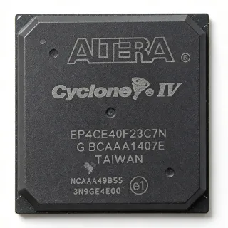
EP2C35F484C6 - Cyclone II FPGA 33K LE 484-FBGA | Intel
MPN: EP2C35F484C6 ✓ Active| Qty | Unit Price | Extended |
|---|---|---|
| 1 | $88.4 | $88.40 |
| 10 | $79.56 | $795.60 |
| 100 | $70.72 | $7,072.00 |
| 500 | $63.5 | $31,750.00 |
| 1,000 | $57.2 | $57,200.00 |
EP2C35F484C6 Overview
A Field-Programmable Gate Array (FPGA) is a type of programmable logic device (PLD) that allows hardware designers to implement arbitrary digital logic functions via a configuration bitstream loaded into on-chip SRAM. FPGAs sit within the broader hierarchy of integrated circuits: programmable logic device -> FPGA -> programmable logic -> digital IC -> semiconductor. They differ from ASICs in that they are reprogrammable after manufacture, and from CPLDs in that they contain much larger amounts of distributed and block memory plus dedicated multiplier blocks.
The Cyclone II architecture integrates embedded 18 x 18 multipliers (35 total), M4K RAM blocks (105 total, 4 Kbit each), and a global clock network with up to 16 PLLs for flexible clock management. Each logic element (LE) contains a 4-input look-up table, a programmable register, and a carry chain, supporting efficient implementation of arithmetic, register, and state-machine logic at speeds up to 250 MHz internal operation. Configuration is supported via active serial (AS), passive serial (PS), and JTAG modes using the dedicated configuration pins.
Typical applications for the EP2C35F484C6 include industrial motor control, video processing pipelines, telecommunications line cards, embedded DSP, and prototyping platforms for ASIC emulation. The 322 user I/O count and 35 dedicated multipliers make it well suited for video buffering and parallel DSP kernels; the low unit cost and Quartus II tool support position it as a mainstream low-cost FPGA for cost-sensitive volume production.
When designing with this part, ensure that the four configuration pins (MSEL[3:0]) are strapped to select the desired configuration mode and that VCCINT (1.2 V) and VCCA (2.5 V PLL analog supply) are decoupled with 0.1 uF ceramic capacitors placed within 100 mils of each supply pin. The device is in production; the Cyclone II family has been the workhorse of low-cost FPGAs since 2004, but Intel now positions Cyclone IV/V/10 as the active roadmap successors.
Drop-in alternatives for EP2C35F484C6 — same package, pin-to-pin compatible. Different-package parts requiring PCB rework are excluded.
Variants in this series
Same-series models that are drop-in compatible with EP2C35F484C6 (same form factor and footprint) — differing in Package, Operating Temperature, Process Technology, Speed Grade, Configuration Modes.
Quick Comparison Tool — Select alternative parts for side-by-side comparison:
EP2C35F484C7N
✅ Drop-In✓ In Stock
$85.2 / Unit
View Datasheet →EP2C35F484C8N
✅ Drop-In✓ In Stock
$65 / Unit
View Datasheet →EP2C35F484I6N
✅ Drop-In✓ In Stock
$52.1 / Unit
View Datasheet →EP2C35F484I7N
✅ Drop-In✓ In Stock
$26.4 / Unit
View Datasheet →EP2C35F484C6N
✅ Drop-In✓ In Stock
$118.2 / Unit
View Datasheet →EP2C35F484I8N
✅ Drop-In✓ In Stock
$56.01 / Unit
View Datasheet →EP2C35F484C6 Maximum Ratings & Electrical Characteristics
| Family | Cyclone II |
| Logic Elements (LE) | 33,216 |
| Embedded Memory Bits | 483,840 bits (105 M4K blocks x 4 Kbit) |
| Embedded 18x18 Multipliers | 35 |
| Maximum User I/O | 322 |
| Process Technology | 90 nm low-k CMOS |
| Core Voltage (VCCINT) | 1.2 V |
| PLL Analog Supply (VCCA) | 2.5 V |
| I/O Standards | LVTTL, LVCMOS (1.5/1.8/2.5/3.3 V), SSTL, HSTL, PCI, differential LVDS, RSDS |
| Package | 484-ball FineLine BGA (FBGA) |
| Speed Grade | -6 |
| Operating Temperature (Commercial) | 0 C to +85 C |
| PLLs | 4 |
| Global Clock Networks | 16 |
| Configuration Modes | Active Serial (AS), Passive Serial (PS), JTAG |
| RoHS Status | Compliant |
| Lead-Free | Yes |
| Mounting Type | Surface Mount (BGA) |
EP2C35F484C6 484-ball fineline bga (fbga) Pin Configuration Guide
Pin configuration for EP2C35F484C6 (484-ball fineline bga (fbga) package). This digital IC includes GPIO, communication interfaces (UART, SPI, I2C), and power pins. Refer to the manufacturer datasheet for alternate pin functions and configuration options. Essential for embedded system design and PCB layout.

No detailed pinout data available for EP2C35F484C6.
Refer to the datasheet for full pin configuration.
Typical Applications
EP2C35F484C6 is suitable for 6 applications: Video Processing and Image Pipeline, Industrial Motor Control, Telecommunications Line Card Interface, Embedded DSP and FIR Filter Banks, ASIC Prototyping and Emulation, Legacy Industrial Control and I/O Aggregation.
Video Processing and Image Pipeline
The EP2C35F484C6 is well matched to mid-resolution video processing where its 33,216 logic elements and 483,840 bits of embedded RAM provide enough capacity for line buffers and color-space conversion. The 35 dedicated 18x18 multipliers handle real-time pixel-rate arithmetic such as scaling, deinterlacing, and motion compensation without consuming general-purpose fabric. Placed on the video capture board between the sensor/decoder and the back-end processor, the FPGA can run a standard ITU-R BT.656 pipeline at 27 MHz or a 720p60 stream at 74.25 MHz with margin on the -6 speed grade. Its 322 user I/O pins allow direct connection to multiple parallel camera inputs and DDR memory buses. Compared with newer Cyclone IV/V devices, EP2C35F484C6 trades higher static power for substantially lower unit cost in mature consumer video products.
Recommended
Industrial Motor Control
Industrial motor control loops require deterministic microsecond-scale response that the EP2C35F484C6 delivers through its 16 global clock networks and four PLLs, supporting multi-axis PWM generation at frequencies above 100 kHz. The 322 user I/O pins accommodate multiple encoder inputs, Hall sensor arrays, and gate-driver interfaces for three-phase IGBT/MOSFET bridges on a single FPGA, replacing multiple dedicated MCU+ASIC stacks. Logic capacity of 33,216 LEs is sufficient for field-oriented control (FOC) state machines, SVPWM modulators, and current-loop PID at rates up to 20 kHz per axis. The 0 to +85 C commercial temperature range covers most indoor cabinet installations, while the industrial-grade EP2C35F484I6N drop-in variant handles outdoor or factory-floor environments.
Recommended
Telecommunications Line Card Interface
Telecommunications line cards commonly use the EP2C35F484C6 to implement protocol bridging between T1/E1 framers, IMA groupings, and Ethernet MACs because the device supports LVDS, LVPECL, and SSTL I/O standards alongside LVCMOS for direct connection to telecom serdes. The 35 multipliers accelerate Reed-Solomon and convolutional codec operations used in forward error correction, while 483,840 bits of RAM buffer packets across clock-domain crossings. Up to 322 user I/O pins accommodate multiple framer/serdes/management interfaces on a single chip, and four PLLs synthesize jitter-cleaned clocks from the system reference. Per Intel's Cyclone II handbook, the LVDS capability supports data rates up to 805 Mbps per channel, sufficient for legacy telecom backplane speeds.
Recommended
Embedded DSP and FIR Filter Banks
Multi-channel audio processing, software-defined radio basebands, and seismic acquisition systems leverage the EP2C35F484C6's 35 hardware 18x18 multipliers to implement FIR and IIR filter banks at sample rates well above 10 MHz. The 18-bit multiplier width supports fixed-point DSP kernels in audio and baseband processing, and the M4K memory blocks can be configured as coefficient ROM tables that are accessed in parallel with each multiply-accumulate operation. 322 user I/O pins allow multiple stereo audio I2S/TDM streams or multiple ADC channels to be aggregated on a single device. The -6 speed grade delivers sufficient setup/hold margin for 200 MHz operation of multiply-accumulate chains without pipelining.
Recommended
ASIC Prototyping and Emulation
ASIC and SoC design teams use the EP2C35F484C6 for RTL prototyping of sub-modules that fit within 33,216 LEs and 483,840 bits of internal memory, particularly peripheral controllers, bus arbiters, and glue logic. Quartus II synthesis maps Verilog/VHDL RTL directly into the fabric with timing-accurate results that closely predict ASIC performance at the pre-layout stage. The 322 user I/O provide ample test-header access for logic-analyzer probing of internal signals via SignalTap II embedded logic analysis. The 484-FBGA package supports high signal-count board-level connections required for multi-FPGA partitioning flows. For larger ASICs, multiple EP2C35F484C6 devices can be cascaded with deterministic inter-chip LVDS links.
Recommended
Legacy Industrial Control and I/O Aggregation
Long-lifecycle industrial systems such as programmable logic controllers, SCADA RTUs, and legacy machine controllers rely on the EP2C35F484C6 to aggregate dozens of 24 V digital inputs, opto-isolated signals, and analog-to-digital converter channels into a single point of control. The 322 user I/O pin count is well matched to mid-density industrial applications where multiple discrete MCUs would otherwise be required, simplifying the BOM and reducing mean-time-between-failure rates. The 0 to +85 C commercial temperature range covers cabinet-mounted installations, and Intel's long-term-of-life commitment to the Cyclone II family ensures multi-decade availability for industrial customers. Quartus II tool support allows IEC 61131-3-style state machines and ladder-logic translation flows to be compiled into the FPGA.
Recommended
Recommended Products Summary
Engineering reference data for EP2C35F484C6 — comparison, design guidance, and compliance information.
Selection Guide
Comparison with Alternatives
| Parameter | This Product | EP2C35F484C7N | EP2C35F484C8N | EP2C35F484I6N | EP2C35F484I7N | EP2C35F484C6N | EP2C35F484I8N |
|---|---|---|---|---|---|---|---|
| Brand | Intel (Altera) | Intel (Altera) | Intel (Altera) | Intel (Altera) | Intel (Altera) | Intel (Altera) | Intel (Altera) |
| Package | 484-ball FineLine BGA (FBGA) | 484-ball FineLine BGA - same | 484-ball FineLine BGA - same | 484-ball FineLine BGA - same | 484-ball FineLine BGA - same | 484-ball FineLine BGA - same | 484-ball FineLine BGA - same |
| Speed Grade | -6 (fastest) | -7 (mid) | -8 (slowest) | -6 | -7 | -6 | -8 |
| Operating Temperature | 0 C to +85 C (Commercial) | 0 C to +85 C (Commercial) | 0 C to +85 C (Commercial) | -40 C to +100 C (Industrial) | -40 C to +100 C (Industrial) | 0 C to +85 C (Commercial) | -40 C to +100 C (Industrial) |
| Logic Elements | 33,216 | 33,216 | 33,216 | 33,216 | 33,216 | 33,216 | 33,216 |
| Embedded RAM (bits) | 483,840 | 483,840 | 483,840 | 483,840 | 483,840 | 483,840 | 483,840 |
| Embedded 18x18 Multipliers | 35 | 35 | 35 | 35 | 35 | 35 | 35 |
| Maximum User I/O | 322 | 322 | 322 | 322 | 322 | 322 | 322 |
| Pin-to-Pin Compatible | Yes (reference) | Yes - drop-in | Yes - drop-in | Yes - drop-in | Yes - drop-in | Yes - drop-in | Yes - drop-in |
Key Differentiators
- Fastest speed grade in 484-FBGA package (vs EP2C35F484C7N)
- Commercial temperature grade for cost-sensitive volume (vs EP2C35F484I6N)
- Identical die to C6N, distinguished by lead-free suffix (vs EP2C35F484C6N)
- Higher logic capacity than Cyclone II EP2C20 family (vs EP2C20F484C8)
Design Notes
Estimated: EP2C35F484C6 quiescent core current at 1.2 V VCCINT is approximately 250 mA for an empty design and scales linearly with toggle rate and logic utilization. At 80% utilization switching at 100 MHz, expect roughly 600-800 mA on VCCINT and 50-100 mA per active I/O bank. Use a low-noise LDO (e.g. LT3080) or a high-efficiency buck regulator followed by an LDO post-regulator to deliver the 1.2 V rail; place 100 uF bulk + 0.1 uF ceramic decoupling within 100 mils of every VCCINT ball. VCCA (2.5 V PLL analog) must be filtered separately from VCCINT to minimize jitter; a ferrite bead + 10 uF + 0.1 uF pi-filter is recommended per Intel's Cyclone II hardware reference design.
The 484-ball FineLine BGA uses a 1.0 mm ball pitch and requires a 4- or 6-layer PCB with microvia (laser-drilled) stack-up for breakout routing. Per the Cyclone II board design guidelines, all VCCINT and GND balls must be connected to internal power planes using full ball-grid-array via-in-pad construction if the board is to meet thermal-via and inductance targets. Use a minimum of 8 ground balls stitched around each PLL region; do not route LVDS signals across split power planes. The exposed die-attach paddle is electrically connected to GND and should be soldered to a central thermal pad with 25+ thermal vias for heat dissipation.
Do not leave MSEL[3:0] floating - strap them to select the configuration mode (00=AS, 01=PS, 10=fast AS, 11=JTAG-only). The nCONFIG pin must be held high through a 10 kohm pull-up to VCCIO of the configuration bank. CONF_DONE must be pulled high externally because it is open-drain. The DCLK line in passive-serial mode must be a clean clock with < 200 ps jitter; running it across noisy switching signals will cause configuration failures. After configuration, dual-purpose configuration pins (e.g., nCEO, nWS, nRS, CS, RDYnBSY, DATA[7:0]) can be re-used as user I/O but only after full user-mode entry - do not toggle them during initialization.
LVDS inputs on Cyclone II require a 100-ohm differential termination across the receiver pair - place the resistor as close to the FPGA balls as possible, ideally within 200 mils. For SSTL and HSTL Class II outputs, reference-voltage (VREF) pins must be bypassed with 0.1 uF + 10 uF capacitance to GND to prevent DC-bias shift during simultaneous switching. Per the Cyclone II device handbook, the maximum supported LVDS data rate is 805 Mbps per channel in commercial grade and 640 Mbps in industrial grade; signal-integrity simulation with the IBIS model is recommended for any channel running above 400 Mbps.
Compliance Information
RoHS and lead-free per Intel/Altera product marking. AEC-Q100 not applicable for commercial/industrial FPGA grade; halogen-free status not stated in provided data.