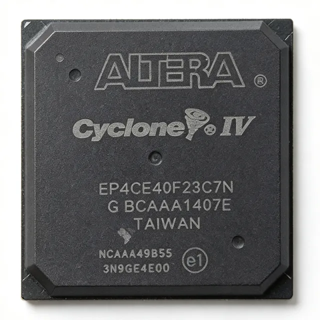
EP4CE40F23C7N - Cyclone IV E FPGA 39.6K LE 484-FBGA | Intel
MPN: EP4CE40F23C7N ✓ Active| Qty | Unit Price | Extended |
|---|---|---|
| 1 | $35.72 | $35.72 |
| 10 | $32.15 | $321.50 |
| 100 | $28.4 | $2,840.00 |
| 500 | $24.95 | $12,475.00 |
| 1,000 | $21.8 | $21,800.00 |
EP4CE40F23C7N Overview
A Field Programmable Gate Array is a semiconductor integrated circuit built around an array of configurable logic blocks (CLBs), programmable interconnect, and dedicated hard IP blocks such as memory and DSP slices. FPGAs occupy the top of the programmable-logic hierarchy alongside CPLDs, with FPGAs typically addressing higher logic densities, on-chip memory, and high-speed serial transceivers for parallel DSP, video, and embedded processing workloads. The Cyclone IV E family is fabricated on a low-power 60 nm process and is optimized for cost-sensitive, high-volume applications.
Key features of the EP4CE40F23C7N include 328 maximum user I/O pins, 4 PLLs for clock management, and 66.5 Kbits of distributed RAM. The device integrates 116 embedded multipliers for DSP workloads, supports external memory interfaces including DDR/DDR2 SDRAM and QDRII SRAM, and provides multiple configuration modes such as JTAG and Active Serial. The 484-FBGA package offers a 1.0 mm ball pitch suitable for multilayer PCB designs.
The Cyclone IV E architecture combines an SRAM-based programmable fabric with hard memory blocks (M9K), DSP blocks (18x18 multipliers), and on-chip PLLs. Compared with the earlier Cyclone III family, Cyclone IV E delivers improved logic utilization, lower static power, and a richer set of I/O standards including LVDS, SSTL, and HSTL for high-speed parallel interfaces.
Typical applications for the EP4CE40F23C7N include industrial motor control and factory automation, video processing and image acquisition, communications protocol bridging, software-defined radio front-ends, and embedded display controllers. The wide I/O count and embedded multipliers make it especially suitable for parallel data acquisition and DSP pipelines.
When designing with this device, ensure proper decoupling with 100 nF and 10 uF capacitors near each power pin, follow Intel's recommended PCB layout guidelines for the FBGA package, and use the Quartus II design software (Cyclone IV E supported edition) for synthesis, place-and-route, and configuration bitstream generation.
This page consolidates distributor pricing, drop-in alternatives from the same Cyclone IV E family, and practical design considerations that go beyond a quick datasheet lookup, helping engineers accelerate part selection and PCB bring-up.
Drop-in alternatives for EP4CE40F23C7N — same package, pin-to-pin compatible. Different-package parts requiring PCB rework are excluded.
Variants in this series
Same-series models that are drop-in compatible with EP4CE40F23C7N (same form factor and footprint) — differing in Package, Speed Grade, Configuration Modes, Process Technology, Embedded Memory.
Quick Comparison Tool — Select alternative parts for side-by-side comparison:
EP4CE40F23C8N
✓ In Stock
$52.95 / Unit
View Datasheet →EP4CE40F23C6N
✓ In Stock
$76.8 / Unit
View Datasheet →EP4CE40F23I7N
✓ In Stock
$52.75 / Unit
View Datasheet →EP4CE40F23A7N
✓ In Stock
$118.4 / Unit
View Datasheet →EP4CE40F23C7
✓ In Stock
$102 / Unit
View Datasheet →EP4CE40F23C7N Maximum Ratings & Electrical Characteristics
| Product Family | Cyclone IV E |
| Logic Elements (LE) | 39,600 |
| Embedded Memory Bits | 1,161,216 bits |
| Embedded 18x18 Multipliers | 116 |
| Maximum User I/O | 328 |
| PLLs | 4 |
| Distributed RAM (Kbits) | 66.5 |
| Process Technology | 60 nm low-power CMOS |
| Core Voltage | 1.2 V (typical) |
| Package | 484-ball FineLine BGA (FBGA) |
| Ball Pitch | 1.0 mm |
| Operating Temperature (Commercial) | 0C to +85C |
| Speed Grade | C7 |
| Configuration Methods | JTAG, Active Serial (AS), Passive Serial (PS) |
| RoHS Status | Compliant |
EP4CE40F23C7N 484-ball fineline bga (fbga) Pin Configuration Guide
Pin configuration for EP4CE40F23C7N (484-ball fineline bga (fbga) package). This digital IC includes GPIO, communication interfaces (UART, SPI, I2C), and power pins. Refer to the manufacturer datasheet for alternate pin functions and configuration options. Essential for embedded system design and PCB layout.

No detailed pinout data available for EP4CE40F23C7N.
Refer to the datasheet for full pin configuration.
Typical Applications
EP4CE40F23C7N is suitable for 6 applications: Industrial Motor Control, Video Processing and Image Acquisition, Communications Protocol Bridging, Software Defined Radio Front-End, Embedded Display Controllers, Test and Measurement Instrumentation.
Industrial Motor Control
The EP4CE40F23C7N's 116 embedded 18x18 multipliers and 39.6K logic elements make it well-suited for field-oriented control (FOC) loops and PWM generation in industrial drives. With 328 user I/Os, the FPGA can directly interface to multiple encoder feedback channels, power-module fault inputs, and high-speed gate-driver signals while running current/torque control loops in the 50-100 kHz range. The on-chip PLLs provide the deterministic clock trees needed for switching frequency synchronization, and the M9K memory blocks buffer ADC sample streams for current sensing. Compared with a DSP+MCU pair, a single EP4CE40 consolidates both control law and custom logic on one die, reducing PCB area and BOM cost for industrial servo and inverter applications.
Recommended
Video Processing and Image Acquisition
With 1.16 Mbits of embedded RAM and 328 I/Os, the EP4CE40F23C7N can capture parallel video streams (e.g. BT.656, LVDS camera link) and perform real-time pixel processing such as color-space conversion, gamma correction, and edge detection. The M9K blocks serve as line buffers for video pipelines, while the 116 hardware multipliers accelerate convolutional kernels and 2D filters at full pixel clock rates. The DDR2 external memory interface enables frame buffering for resolutions up to 1080p, and the 4 PLLs generate independent pixel clocks for capture and display paths. Compared with ASSP video processors, the FPGA offers post-deployment upgradeability for new image-processing algorithms without silicon change.
Recommended
Communications Protocol Bridging
The EP4CE40F23C7N's 328 I/Os support simultaneous multi-protocol bridging - for example, UART/SPI/I2C to Ethernet, or CAN-FD to USB - by instantiating multiple soft IP cores in parallel on the FPGA fabric. The 4 on-chip PLLs synthesize the independent clocks each protocol requires (e.g. 25 MHz for Ethernet PHY, 48 MHz for USB), and the 116 multipliers handle CRC and encryption offload. With 1.16 Mbits of embedded memory, packet buffers fit entirely on-chip for sub-millisecond latency, eliminating the need for external SRAM in small-form-factor bridge designs. Industrial temperature variants of the same die enable deployment in factory-floor gateways.
Recommended
Software Defined Radio Front-End
The EP4CE40F23C7N's 116 dedicated 18x18 multipliers enable baseband signal processing for narrowband SDR applications such as digital amateur radio, low-power telemetry, and industrial wireless links. DDC/DUC (digital down/up conversion) and FIR filtering run in real time at sample rates up to ~50 MSPS using the multiplier array, while the embedded memory holds NCO lookup tables and channelizer coefficients. The 328 I/Os accommodate dual ADC/DAC interfaces plus a parallel host bus, and the PLLs synthesize the multiple sample-rate clocks needed for IF and baseband. Compared with a general-purpose DSP, the FPGA fabric delivers deterministic latency critical for time-sensitive protocol stacks.
Recommended
Embedded Display Controllers
The EP4CE40F23C7N can drive TFT LCD panels and HDMI/DVI encoders through its 328 I/Os, providing timing controller, color-depth conversion, and on-screen display (OSD) overlay functions. The M9K memory blocks implement frame-buffer queues, while the 4 PLLs generate pixel clocks up to 148.5 MHz for 1080p60 output. The 116 embedded multipliers accelerate JPEG decode for OSD sprite rendering. With the DDR2 interface, the FPGA can buffer a full 1080p frame externally, and the commercial temperature grade (0C to 85C) covers most indoor and protected-outdoor display applications.
Recommended
Test and Measurement Instrumentation
The EP4CE40F23C7N provides the logic density and I/O count needed to build custom data-acquisition front-ends, protocol analyzers, and logic-analyzer probes. The 116 multipliers enable real-time DSP pre-processing (FIR filtering, decimation) on incoming samples before forwarding to a host PC, while the 1.16 Mbits of embedded memory serve as circular sample buffers. The on-chip PLLs synthesize multiple sample-rate clocks from a single reference, and the JTAG configuration interface allows rapid firmware iteration during test development. The commercial temperature grade is sufficient for bench-instrument use; the industrial variants extend deployment to factory test cells.
Recommended
Recommended Products Summary
Engineering reference data for EP4CE40F23C7N — comparison, design guidance, and compliance information.
Selection Guide
Comparison with Alternatives
| Parameter | This Product | EP4CE40F23C8N | EP4CE40F23C6N | EP4CE40F23I7N | EP4CE40F23A7N | EP4CE40F23C7 |
|---|---|---|---|---|---|---|
| Package | 484-FBGA (F23), 1.0 mm pitch | 484-FBGA (F23) - same | 484-FBGA (F23) - same | 484-FBGA (F23) - same | 484-FBGA (F23) - same | 484-FBGA (F23) - same |
| Brand | Intel (formerly Altera) | Intel - same | Intel - same | Intel - same | Intel - same | Intel - same |
| Logic Elements | 39,600 | 39,600 | 39,600 | 39,600 | 39,600 | 39,600 |
| Speed Grade | C7 | C8 (slower) | C6 (faster) | I7 | A7 | C7 - same |
| Operating Temperature | 0C to +85C (Commercial) | 0C to +85C | 0C to +85C | -40C to +100C (Industrial) | -40C to +125C (Automotive) | 0C to +85C |
| User I/O (max) | 328 | 328 | 328 | 328 | 328 | 328 |
| Embedded Multipliers (18x18) | 116 | 116 | 116 | 116 | 116 | 116 |
| AEC-Q100 Qualified | No | No | No | No | Yes (Automotive) | No |
Key Differentiators
- Highest user I/O count in the EP4CE40 family (vs EP4CE40F29 (variant with different BGA))
- Cyclone IV E cost-optimized process node (vs Cyclone V E (5CEBA4) in similar logic range)
- Speed grade C7 for typical industrial timing closure (vs EP4CE40F23C8N (C8 speed grade))
Design Notes
The 484-ball FBGA package with 1.0 mm pitch requires 4 to 6 layer PCB stack-up with controlled-impedance traces. Per the Cyclone IV E device handbook, route all decoupling capacitors (100 nF and 10 uF) within 100 mils of each VCCINT, VCCA, and VCCIO power pin. Use a continuous ground plane on layer 2 directly under the BGA to minimize return-path inductance, and via-in-pad is recommended for the inner rows of balls.
The EP4CE40F23C7N requires multiple supply rails: VCCINT (1.2 V core), VCCA (2.5 V PLL analog), VCCIO (1.2 V to 3.3 V I/O banks), and VCCPD (3.3 V configuration). Power sequencing per Intel's specification requires VCCINT and VCCA to ramp before or simultaneously with VCCIO; failure to follow the sequence can latch-up the device. Estimate: at 50% toggle rate with all I/O active, ICCINT is roughly 500 mA, so the 1.2 V regulator should deliver at least 1 A headroom.
Estimated: with the FBGA-484 package, theta_JA is approximately 12 C/W on a JEDEC 4-layer test board with adequate copper. At full DSP utilization (116 multipliers @ 200 MHz) plus 50% LE toggle, junction power is roughly 1.5-2.0 W, giving a junction temperature rise of 18-24 C above ambient. For enclosed industrial environments where ambient reaches 70 C, design for airflow or attach a small heatsink to keep Tj below 100 C for reliability margin.
Do not leave unused I/O banks floating - configure them as inputs with internal weak pull-ups or as outputs driving known values, or they may draw extra current and inject noise. The configuration pins (MSEL[3:0], nCE, nCONFIG, nSTATUS, CONF_DONE) require specific pull-up/pull-down values per the configuration mode selected - mixing them up causes configuration failure. Always include a JTAG header for in-system programming and debugging.
Compliance Information
RoHS and REACH compliant per Intel Cyclone IV E product page. Standard C7 commercial part is not AEC-Q100 qualified - choose EP4CE40F23A7N for automotive applications.
