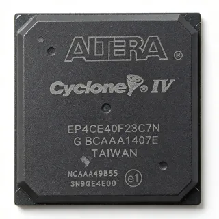
EP2S30F484I4N - Stratix II FPGA 33.8K LE | Intel | BGA-484
MPN: EP2S30F484I4N ✗ End of Life| Qty | Unit Price | Extended |
|---|---|---|
| 1 | $425 | $425.00 |
| 10 | $395 | $3,950.00 |
| 100 | $360 | $36,000.00 |
| 500 | $330 | $165,000.00 |
| 1,000 | $305 | $305,000.00 |
EP2S30F484I4N Overview
A field-programmable gate array (FPGA) is a type of programmable logic IC whose interconnect, logic, and I/O can be configured by the end user after manufacture. FPGAs occupy a middle ground between fixed-function ASICs and software-programmable processors: faster and more deterministic than microcontrollers for parallel DSP tasks, but lower NRE cost than ASICs at low volumes. Within the wider semiconductor hierarchy, an FPGA belongs to the programmable logic category, which sits under digital ICs and is itself a sub-category of integrated circuits. The Stratix II family in particular positioned itself between mid-range FPGAs and high-end DSP platforms, with embedded multipliers and TriMatrix memory blocks optimised for parallel data paths.
Key features of the EP2S30F484I4N include 33,880 logic elements, 1,369,728 bits of on-chip RAM distributed across TriMatrix memory blocks, up to 342 user I/Os (the verified listing states 342), an industrial temperature grade, and a RoHS-compliant lead-free finish. The 484-pin BGA footprint with 1.0 mm ball pitch is designed for high-speed signalling and dense board layouts. The 'N' suffix indicates that the device is lead-free and RoHS compliant, while 'I4' places the device in the -40C to +100C industrial temperature range.
The Stratix II architecture introduces the ALM, which contains a fracturable lookup table, two adders, and a register, giving better utilisation than the older 4-input LUT architecture. Dedicated DSP blocks support 9x9, 18x18, and 36x36 multipliers without consuming general logic. Combined with embedded transceivers (where present on the device variant) and on-chip PLLs, this allows Stratix II designs to deliver several hundred MHz of DSP throughput and multi-gigabit serial I/O on a single die.
Typical applications include high-speed digital signal processing in communications infrastructure, ASIC prototyping and emulation, video and image processing pipelines, high-performance computing acceleration, and military/aerospace signal processing. The industrial temperature grade extends suitability to outdoor base stations, factory automation controllers, and avionics subsystems where wide thermal margin is mandatory.
When designing with this device, ensure PCB layout supports the 1.0 mm BGA pitch with appropriate via-in-pad or microvia construction. Power integrity requires multiple decoupling rails because Stratix II parts separate core, I/O, PLL, and transceiver supplies. Quartus II design software is the primary toolchain; legacy projects may require version pinning because the device family is end-of-life.
This page synthesizes distributor stock and pricing, drop-in same-package alternatives drawn from the Stratix II family, and practical design notes not found in the manufacturer datasheet, providing unique procurement and engineering value beyond what is available on any single distributor page.
Drop-in alternatives for EP2S30F484I4N — same package, pin-to-pin compatible. Different-package parts requiring PCB rework are excluded.
Variants in this series
Same-series models that are drop-in compatible with EP2S30F484I4N (same form factor and footprint) — differing in Speed Grade, Package, Operating Temperature, Core Voltage, PLLs.
Quick Comparison Tool — Select alternative parts for side-by-side comparison:
EP2S30F484I4
✅ Drop-In✓ In Stock
$159 / Unit
View Datasheet →EP2S30F484C5N
✅ Drop-In✓ In Stock
$367.48 / Unit
View Datasheet →EP2S30F484C5
✅ Drop-In✓ In Stock
$305.4 / Unit
View Datasheet →EP2S30F484C4N
✅ Drop-In✓ In Stock
$480 / Unit
View Datasheet →EP2S30F484C4
✅ Drop-In✓ In Stock
$124 / Unit
View Datasheet →EP2S30F484C3N
✅ Drop-In✓ In Stock
$797.9622 / Unit
View Datasheet →EP2S30F484C3
✅ Drop-In✓ In Stock
$620 / Unit
View Datasheet →EP2S30F484I4N Maximum Ratings & Electrical Characteristics
| Family | Stratix II |
| Logic Elements | 33,880 |
| Embedded Memory | 1,369,728 bits |
| User I/O Pins | 342 |
| Package | 484-ball FineLine BGA (FBGA) |
| Ball Pitch | 1.0 mm |
| Process Technology | 90 nm |
| Core Voltage | 1.2 V (refer to datasheet) |
| Operating Temperature Grade | Industrial -40C to +100C |
| Lead-Free / RoHS | Yes (N suffix indicates lead-free RoHS) |
| Speed Grade | 4 |
| On-Chip DSP Blocks | Yes (dedicated 9x9/18x18/36x36 multipliers) |
| PLLs | Yes (on-chip, refer to datasheet for count) |
| Configuration Method | Serial/parallel via Quartus II |
| Mounting Type | Surface Mount (BGA) |
EP2S30F484I4N 484-ball fineline bga (fbga) Pin Configuration Guide
Pin configuration for EP2S30F484I4N (484-ball fineline bga (fbga) package). This digital IC includes GPIO, communication interfaces (UART, SPI, I2C), and power pins. Refer to the manufacturer datasheet for alternate pin functions and configuration options. Essential for embedded system design and PCB layout.

No detailed pinout data available for EP2S30F484I4N.
Refer to the datasheet for full pin configuration.
Typical Applications
EP2S30F484I4N is suitable for 6 applications: Telecom Baseband and DSP, ASIC Prototyping and Emulation, Video and Image Processing, Military and Aerospace Signal Processing, High-Performance Computing Acceleration, Industrial Automation and Control.
Telecom Baseband and DSP
The EP2S30F484I4N suits telecom baseband and DSP applications because its 33,880 logic elements and dedicated 9x9, 18x18, and 36x36 multiplier blocks deliver hundreds of MMACs of DSP throughput per device. The Stratix II ALM architecture maps FIR filters, FFT engines, and channel cards efficiently. With 342 user I/Os, the part can connect to external DDR/QDR memory and multiple SFP/SerDes links simultaneously, while the industrial -40C to +100C temperature grade supports outdoor base-station enclosures. Place 1.2V core and 3.3V I/O rails on isolated planes to meet Stratix II power-integrity guidelines and use Quartus II 13.1 for synthesis and place-and-route.
Recommended
ASIC Prototyping and Emulation
The EP2S30F484I4N is well-suited to ASIC prototyping because the 33,880 logic elements and 1,369,728 bits of TriMatrix memory allow multi-million-gate ASIC designs to be partitioned across one or more Stratix II devices. The 484-ball FBGA package exposes 342 user I/Os for inter-FPGAs cabling and live stimulus injection. The industrial temperature grade suits bench and chassis environments with limited cooling. Timing closure is achieved with Quartus II 13.1 TimeQuest, and the part supports multi-FPGA configuration via JTAG or passive serial. Memory blocks emulate SRAM/DRAM traffic patterns for early firmware development before silicon is available.
Recommended
Video and Image Processing
The EP2S30F484I4N accelerates video pipelines because the on-chip DSP blocks and TriMatrix memory combine to sustain real-time pixel throughput for 1080p60 and beyond. Designers implement motion estimation, deinterlacing, scaling, and colour-space conversion in hardware. The 342 user I/Os connect to HDMI/DVI/MIPI bridges and external DDR2 buffers. The ALM architecture supports both LUT-intensive pixel manipulation and register-heavy line buffers. Industrial temperature enables industrial camera and broadcast equipment deployments. Pair with EP2S15F484 family members for multi-board designs that scale processing capacity.
Recommended
Military and Aerospace Signal Processing
The EP2S30F484I4N operates over -40C to +100C with full industrial qualification, making it a candidate for military and aerospace signal-processing payloads where extended thermal margins are mandatory. Applications include radar IF processing, software-defined radio baseband, and electronic-warfare subsystems. The Stratix II ALM and dedicated DSP blocks deliver deterministic latency required for phased-array beamforming and pulse compression. Designers should review latest MIL-STD-810 and MIL-STD-1540 environmental reports and lock to a specific Quartus II 13.1 service pack for design reproducibility across long programme lifecycles.
Recommended
High-Performance Computing Acceleration
The EP2S30F484I4N accelerates compute kernels in high-performance computing because its 33,880 logic elements run massively parallel algorithms that CPUs cannot sustain. Examples include genomics alignment, financial Monte Carlo simulation, and scientific FFT/IQ transforms. The 1,369,728 bits of TriMatrix memory hold large lookup tables and partial sums, while 342 I/Os feed PCIe or serial RapidIO host links. Industrial temperature allows deployment in accelerator blades and edge-compute nodes. Migrating to newer Stratix/Cyclone families reduces power, but legacy HPC installations still depend on Stratix II for software compatibility.
Recommended
Industrial Automation and Control
The EP2S30F484I4N is used in industrial automation because its industrial -40C to +100C temperature grade withstands factory-floor conditions, motor-drive cabinets, and outdoor process plants. The 33,880 logic elements and DSP blocks execute multi-axis motion control, EtherCAT/PROFIBUS protocol bridging, and high-speed deterministic logic. The 342 user I/Os connect to incremental encoders, sigma-delta ADCs, and isolated RS-485/232 links. Lead-free RoHS-compliant finish (N suffix) supports modern factory environmental directives. Pair with EP2C35F484 or EP2C50F484 Cyclone II devices for cost-optimised auxiliary controllers.
Recommended
Recommended Products Summary
Engineering reference data for EP2S30F484I4N — comparison, design guidance, and compliance information.
Selection Guide
Comparison with Alternatives
| Parameter | This Product | EP2S30F484I4 | EP2S30F484C5N | EP2S30F484C5 | EP2S30F484C4N | EP2S30F484C4 | EP2S30F484C3N | EP2S30F484C3 |
|---|---|---|---|---|---|---|---|---|
| Brand | Intel (formerly Altera) | Intel (formerly Altera) | Intel (formerly Altera) | Intel (formerly Altera) | Intel (formerly Altera) | Intel (formerly Altera) | Intel (formerly Altera) | Intel (formerly Altera) |
| Package | 484-ball FBGA (F484) | 484-ball FBGA (F484) - same | 484-ball FBGA (F484) - same | 484-ball FBGA (F484) - same | 484-ball FBGA (F484) - same | 484-ball FBGA (F484) - same | 484-ball FBGA (F484) - same | 484-ball FBGA (F484) - same |
| Logic Elements | 33,880 | 33,880 | 33,880 | 33,880 | 33,880 | 33,880 | 33,880 | 33,880 |
| Embedded Memory | 1,369,728 bits | 1,369,728 bits | 1,369,728 bits | 1,369,728 bits | 1,369,728 bits | 1,369,728 bits | 1,369,728 bits | 1,369,728 bits |
| User I/O | 342 | 342 | 342 | 342 | 342 | 342 | 342 | 342 |
| Temperature Grade | Industrial -40C to +100C | Industrial -40C to +100C | Commercial 0C to +85C | Commercial 0C to +85C | Commercial 0C to +85C | Commercial 0C to +85C | Commercial 0C to +85C | Commercial 0C to +85C |
| Speed Grade | 4 (I4) | 4 (I4) | 5 (faster) | 5 (faster) | 4 | 4 | 3 (slower) | 3 (slower) |
| Lead-Free (RoHS) | Yes (N suffix) | No (leaded finish) | Yes (N suffix) | No (leaded finish) | Yes (N suffix) | No (leaded finish) | Yes (N suffix) | No (leaded finish) |
Key Differentiators
- Industrial temperature grade with same die as commercial parts (vs EP2S30F484C5N)
- Lead-free RoHS-compliant finish for modern assemblies (vs EP2S30F484I4)
- Speed grade 4 balances timing closure and power (vs EP2S30F484C3N)
Design Notes
The 484-ball FBGA at 1.0 mm pitch requires via-in-pad or microvia PCB technology for reliable assembly. Use 0.5 mm drill microvias with 1.0 mm pad diameter and stagger the via pattern to avoid solder voids. Assign at least four inner layers to GND planes for return-path continuity, and place 0.1uF X7R decoupling capacitors on every eight power pins within 5 mm of the BGA. A 4-layer stack-up with 1 oz copper is acceptable for prototype; production typically moves to 6-8 layers with 2 oz copper on inner planes to handle the 1.2V core current transients.
Stratix II devices require multiple isolated supply rails: 1.2V core, 2.5V/3.3V I/O, 2.5V analog, and 1.2V PLL supplies. Each rail needs its own bulk capacitor bank of 220-470uF low-ESR polymer or tantalum plus 10uF and 0.1uF ceramic decoupling distributed under the BGA. Estimated: at 100% resource utilisation with 200 MHz logic, total core current reaches approximately 2-3 A; I/O banks can draw another 1-2 A. Use a sequencer such as the LTC2923 to enforce 1.2V core before 3.3V I/O ramp-up to avoid latch-up. Verify sequencing in the Quartus II 13.1 power analyser early in the design cycle.
Do not migrate from EP2S30F484I4N to a non-484-ball variant such as EP2S30F672C3N without PCB rework - the F672 FBGA-672 has a completely different footprint and pin map. Estimated: PCB redesign, re‑spin, and qualification for a Stratix II migration can add 8-12 weeks to a project. For volume production, design two PCB footprints (FBGA-484 and FBGA-672) from day one. Always verify the latest Intel/Altera PCN (product-change-notification) database before committing to a last-time buy, because Stratix II is end-of-life and last shipments may have updated substrates.
High-speed differential pairs on Stratix II should be routed with 100 ohm differential impedance, 4-8 mil trace width on outer microstrip layers, and length-matching within 5 mils for LVDS and within 25 mils for DDR2. Keep high-speed traces away from the BGA power vias by at least 3W (where W is trace width). Use the Quartus II 13.1 pin planner to assign I/O banks before final layout, because once a bank voltage is set, all eight I/O standards in that bank share that supply. Reference Intel/Altera application note AN-356 for detailed Stratix II layout guidance.
Compliance Information
RoHS compliance and lead-free finish verified by N suffix in MPN and confirmed in distributor listings (DigiKey). Halogen-free and conflict-minerals status not provided in verified data - left as 'unknown' rather than guessed. AEC-Q100 not applicable to FPGAs of this family; refer to specific automotive variant if required.