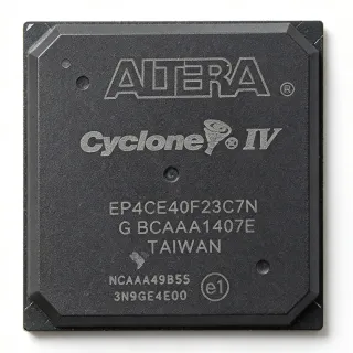
EP2C20F484C6 - Cyclone II FPGA 18,752 LE 484-FBGA | Intel
MPN: EP2C20F484C6 ✗ End of Life| Qty | Unit Price | Extended |
|---|---|---|
| 1 | $100.48 | $100.48 |
| 10 | $90.43 | $904.30 |
| 100 | $80.39 | $8,039.00 |
| 500 | $72.85 | $36,425.00 |
| 1,000 | $65.31 | $65,310.00 |
EP2C20F484C6 Overview
A field-programmable gate array (FPGA) is a programmable logic device that combines configurable logic blocks (LBs/LABs), programmable interconnects, and dedicated I/O cells on a single silicon die. In the broader component taxonomy, an FPGA sits under programmable logic -> digital logic -> semiconductor IC. The Cyclone II family targets cost-sensitive, high-volume applications such as industrial control, video processing, and communication bridges, offering ASIC-like integration without the NRE cost. The "EP2C20" prefix encodes family and logic capacity; the "F484" suffix identifies the 484-pin fine-line BGA package, while "C6" denotes the commercial speed grade (slowest, lowest power).
Key features include up to 500 MHz internal operation, support for multiple I/O standards (LVTTL, LVCMOS, PCI, SSTL, LVDS), four phase-locked loops (PLLs) for clock management, and a 1.2 V core supply with multi-voltage I/O banks (1.5 V, 1.8 V, 2.5 V, 3.3 V). The Cyclone II architecture is SRAM-based, so an external configuration memory is mandatory at every power-up. Because the part is mature, it has been widely adopted in long-lifecycle industrial designs and university teaching labs.
Typical applications include motor-control and servo drive logic in factory automation, video-format conversion and scaling engines, low-cost software-defined peripherals over PCIe, display controllers and LCD drivers, automotive infotainment prototypes, and education platforms for HDL training. Compared with newer Cyclone IV/V devices, EP2C20F484C6 trades lower static power for older I/O and PLLs, but retains the lowest unit cost in the legacy Cyclone family.
When designing with EP2C20F484C6, ensure the JTAG chain is correctly buffered and the configuration flash is sized for at least 8 Mbit. The 484-FBGA requires careful PCB layout with via-in-pad microvias and matched-length impedance-controlled traces for DDR or LVDS channels. Refer to the Cyclone II Device Handbook (Section I, Cyclone II Data Sheet) for IO-bank restriction and termination guidelines.
This page synthesizes distributor pricing, drop-in alternatives in the same 484-FBGA footprint, and practical PCB-layout notes not duplicated in the manufacturer datasheet, providing design engineers with the cross-reference depth needed for legacy Cyclone II BOM management.
Drop-in alternatives for EP2C20F484C6 — same package, pin-to-pin compatible. Different-package parts requiring PCB rework are excluded.
Variants in this series
Same-series models that are drop-in compatible with EP2C20F484C6 (same form factor and footprint) — differing in Speed Grade, Package, Process Technology, Operating Temperature, RoHS Status.
Quick Comparison Tool — Select alternative parts for side-by-side comparison:
EP2C20F484C6N
✅ Drop-In✓ In Stock
$68.1 / Unit
View Datasheet →EP2C20F484C8N
✅ Drop-In✓ In Stock
$23.95 / Unit
View Datasheet →EP2C20F484I6N
✅ Drop-In ⚠️ 参数待验证✓ In Stock
$47.85 / Unit
View Datasheet →EP2C20F484C7N
✅ Drop-In ⚠️ 参数待验证✓ In Stock
$42.5 / Unit
View Datasheet →EP2C20F484C8
✅ Drop-In✓ In Stock
$22.2 / Unit
View Datasheet →EP2C20F484I8N
✅ Drop-In ⚠️ 参数待验证✓ In Stock
$49.1 / Unit
View Datasheet →EP2C20F484C6 Maximum Ratings & Electrical Characteristics
| Family | Cyclone II |
| Logic Elements | 18,752 |
| Logic Array Blocks (LABs) | 1,172 |
| Embedded 18x18 Multipliers | 117 |
| Total RAM Bits | 239,616 |
| M4K Memory Blocks | 26 (typical) |
| Maximum User I/O | 315 |
| PLLs | 4 |
| Operating Frequency | up to 500 MHz |
| Core Voltage | 1.2 V |
| I/O Bank Voltages | 1.5 V / 1.8 V / 2.5 V / 3.3 V |
| Process Technology | 90 nm TSMC |
| Package | 484-ball FineLine BGA (FBGA) |
| Speed Grade | C6 (commercial, slowest) |
| Operating Temperature | 0 C to +85 C (commercial) |
| Configuration Mode | Active Serial (AS) / Passive Serial (PS) / JTAG |
| RoHS Status | Compliant (lead-free) |
EP2C20F484C6 484-ball fineline bga (fbga) Pin Configuration Guide
Pin configuration for EP2C20F484C6 (484-ball fineline bga (fbga) package). This digital IC includes GPIO, communication interfaces (UART, SPI, I2C), and power pins. Refer to the manufacturer datasheet for alternate pin functions and configuration options. Essential for embedded system design and PCB layout.

No detailed pinout data available for EP2C20F484C6.
Refer to the datasheet for full pin configuration.
Typical Applications
EP2C20F484C6 is suitable for 6 applications: Industrial Motor Drive Controllers, Video Format Conversion and Scaling, PCIe Endpoint Bridge for Low-Cost Systems, Display Controller and LCD Panel Driver, Software-Defined Radio Front-End Processing, Education and HDL Training Platforms.
Industrial Motor Drive Controllers
The EP2C20F484C6 is widely adopted in industrial motor-control designs because its 18,752 logic elements and 117 dedicated 18x18 multipliers are well-matched to field-oriented control (FOC) algorithms and PWM generation for three-phase inverters. The four on-chip PLLs provide the deterministic clock tree required to synchronize PWM outputs with encoder feedback, while 315 user I/Os support multiple encoder interfaces, gate-driver enable signals, and CAN/RS-485 comms. Built-in M4K blocks hold sinusoidal and Clarke/Park transform tables for real-time torque control. Compared with a discrete MCU plus DSP approach, a Cyclone II consolidates the entire control loop on one device.
Recommended
Video Format Conversion and Scaling
The EP2C20F484C6's combination of 18,752 LEs, 239,616 RAM bits, and LVDS-capable I/O banks makes it a strong fit for video-processing bridges between cameras, LCD panels, and HDMI/DVI sinks. Embedded M4K blocks can hold two full video lines for polyphase scaling or color-space conversion at 1080p60, and the four PLLs generate the precise pixel clocks required for SDI/DVI serializers. Engineers typically pair this device with an external HDMI transmitter such as the ADV7513 and a video ADC for legacy analog inputs. The 484-FBGA package allows clean breakout of LVDS pairs to HDMI connectors on standard 4-layer PCBs.
Recommended
PCIe Endpoint Bridge for Low-Cost Systems
Implementing a single-lane PCIe Gen1 endpoint in the EP2C20F484C6 consumes roughly 3,000 LEs and one PLL, leaving ample room for custom application logic. Hard IP for PCIe is not present in Cyclone II, so designers implement the PHY in soft logic and pair the FPGA with an external PCIe clock buffer. The device's 315 user I/Os and 26 M4K blocks provide abundant FIFO storage for DMA engines, while the 484-FBGA ballout cleanly routes the PCIe transmit/receive pairs and reference clock. This is a common architecture in low-cost data-acquisition cards and FPGA-based prototyping platforms.
Recommended
Display Controller and LCD Panel Driver
The EP2C20F484C6 drives large TFT LCD panels by generating the timing controller (TCON) signals and buffering pixel data through internal M4K RAM in the 484-FBGA package. Its LVDS I/O banks support direct connection to flat-panel displays with up to 24-bit color depth, and the four PLLs produce the pixel clock, gate-driver shift clock, and source-driver data clock from a single low-cost crystal. Designers often implement PIP (picture-in-picture), OSD (on-screen display), and gamma-correction logic in unused LEs. Compared with a discrete LCD controller ASIC, the FPGA offers in-field firmware upgrades for new panel resolutions.
Recommended
Software-Defined Radio Front-End Processing
The EP2C20F484C6 is used as a digital down-conversion and channelization stage in low-cost software-defined radio platforms. Its 117 18x18 multipliers implement NCOs and digital filters at IF bandwidths up to 80 MHz, while the M4K blocks serve as data buffers between the ADC and a host processor. The four PLLs generate the ADC sampling clock and DSP clock from a single TCXO reference, achieving sub-100 ps jitter suitable for narrowband FM and digital modes. Its 315 I/Os interface to parallel ADCs such as the AD9248 and high-speed LVDS data converters.
Recommended
Education and HDL Training Platforms
Universities and training labs use the EP2C20F484C6 in development boards such as the Altera DE2 because its 18,752 LEs provide enough headroom for medium-complexity student projects while remaining affordable at single-unit pricing. Quartus II Web Edition (free) supports the device, and the 484-FBGA package breaks out to commonly used peripherals (VGA, PS/2, Ethernet PHY, audio codec). Students learn timing closure, PLL configuration, and on-chip memory inference without the cost of cutting-edge silicon. The Cyclone II legacy status means older boards are abundant on the secondary market.
Recommended
Recommended Products Summary
Engineering reference data for EP2C20F484C6 — comparison, design guidance, and compliance information.
Selection Guide
Comparison with Alternatives
| Parameter | This Product | EP2C20F484C6N | EP2C20F484C8N | EP2C20F484I6N | EP2C20F484C7N | EP2C20F484C8 | EP2C20F484I8N |
|---|---|---|---|---|---|---|---|
| Brand | Intel | Intel | Intel | Intel | Intel | Intel | Intel |
| Package | 484-FBGA | 484-FBGA (same) | 484-FBGA (same) | 484-FBGA (same) | 484-FBGA (same) | 484-FBGA (same) | 484-FBGA (same) |
| Speed Grade | C6 | C6 (same) | C8 (faster) | C6 industrial | C7 (mid) | C8 (faster, lead) | C8 industrial |
| Logic Elements | 18,752 | 18,752 (same die) | 18,752 (same die) | 18,752 (same die) | 18,752 (same die) | 18,752 (same die) | 18,752 (same die) |
| User I/O Count | 315 | 315 | 315 | 315 | 315 | 315 | 315 |
| Temperature Range | 0 to +85 C (Commercial) | 0 to +85 C | 0 to +85 C | -40 to +100 C (Industrial) | 0 to +85 C | 0 to +85 C | -40 to +100 C (Industrial) |
| RoHS / Lead-Free | Lead-bearing (non-RoHS variant) | Lead-free RoHS | Lead-free RoHS | Lead-free RoHS | Lead-free RoHS | Lead-bearing (non-RoHS) | Lead-free RoHS |
| Lifecycle Status | NRND | NRND | NRND | NRND | NRND | NRND | NRND |
Key Differentiators
- RoHS-compliant lead-free production variant (vs EP2C20F484C6)
- Higher internal performance via C8 speed grade (vs EP2C20F484C6 (C6))
- Industrial temperature range for harsh environments (vs EP2C20F484C6 (commercial 0 to +85 C))
Design Notes
The 484-FBGA uses a 1.0 mm ball pitch and demands 4 to 6 PCB layers with microvia-in-pad (or staggered microvias) on inner escape layers. Power planes (1.2 V core, 2.5/3.3 V I/O) must be split carefully because the device has eight I/O banks each with independent VCCIO pins; a missing decoupling cap on any bank can cause PLL jitter or LVDS eye closure. Plan for at least 12 low-ESR 0402/0603 ceramic decoupling capacitors around the device, plus a 100 uF bulk cap per rail.
Core current draw on EP2C20F484C6 can exceed 1.5 A at 500 MHz with all PLLs active. Use a switching regulator with at least 3 A capability and a ferrite bead plus 10 uF bulk cap at the FPGA supply pin to suppress switching noise. Estimate: a TPS54331 at 1.2 V/3 A is a typical reference design choice. Keep the analog PLL supply VCC_PLL separate from the digital 1.2 V rail, with its own pi-filter.
Route LVDS pairs as 100 ohm differential with matched length within 150 mil and 90 degree bends avoided. JTAG pins (TCK, TMS, TDI, TDO) need a 4.7 kohm pull-up on TCK and a 10 kohm pull-up on TMS/TDI for reliable configuration in AS mode. Place the 50 MHz configuration reference crystal within 100 mil of the CLKUSR pin and guard it with a GND ring to avoid coupling from switching I/O.
Do not leave MSEL[3:0] floating - they select the configuration mode (AS, PS, JTAG, Fast AS) and must be tied high or low per the datasheet. The Cyclone II does not support multi-voltage I/O without correct VCCIO per bank; mixing 1.5 V and 3.3 V signals on the same bank will damage I/O cells. Also note that 90 nm SRAM-based FPGAs require a configuration bitstream at every power-up - loss of configuration memory is silent and can cause field returns if the EPCS flash is undersized.
Compliance Information
EP2C20F484C6 is the lead-bearing variant and is NOT RoHS compliant. For RoHS-compliant applications in 2026, choose EP2C20F484C6N (same die, lead-free BGA balls). REACH compliance is per Intel product page. AEC-Q100 is not applicable (this is not an automotive-qualified part; commercial/industrial grades only).