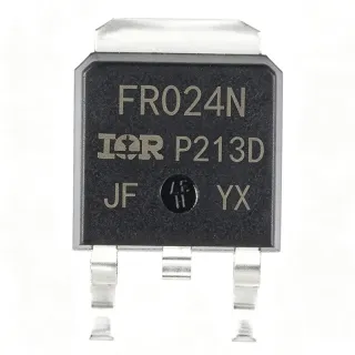
IRFR3710ZTRPBF - 100V N-Channel 56A HEXFET MOSFET | Infineon
MPN: IRFR3710ZTRPBF ✓ Active| Qty | Unit Price | Extended |
|---|---|---|
| 1 | $0.86 | $0.86 |
| 10 | $0.74 | $7.40 |
| 100 | $0.62 | $62.00 |
| 500 | $0.55 | $275.00 |
| 1,000 | $0.48 | $480.00 |
| 2,500 | $0.42 | $1,050.00 |
IRFR3710ZTRPBF Overview
A power MOSFET is a voltage-controlled semiconductor switch that uses the gate field effect to modulate current flow between the drain and source terminals. Within the discrete semiconductor taxonomy, MOSFETs belong to the field-effect transistor family and serve as the fundamental building block of switched-mode power supplies, motor drives, and synchronous rectification stages. The DPAK (TO-252AA) package is one of the most widely adopted surface-mount outlines for medium-power MOSFETs because its exposed thermal pad provides a low thermal resistance path while keeping the PCB footprint compact.
Key features of the IRFR3710ZTRPBF include a 175 °C maximum junction operating temperature for high ambient or pulsed-power environments, fast switching speed suitable for high-frequency converters, an improved repetitive avalanche rating for inductive load switching, and a logic-level-friendly 10 V VGS(th) typical gate threshold. The low RDS(on) of 18 mOhm directly reduces conduction losses and improves thermal performance in continuous-current paths such as low-side switches and synchronous rectifiers.
Architecturally, the device uses Infineon's HEXFET cell structure, a planar/vertical DMOS design optimized for low figure-of-merit (RDS(on) × Qg) and rugged avalanche capability. This combination delivers strong efficiency in hard-switched topologies and resilience against voltage transients induced by motor windings or transformer leakage inductance.
Typical applications include DC-DC buck/boost converters, synchronous rectification in isolated power supplies, motor drive H-bridges, solenoid and relay drivers, battery protection circuits, and hot-swap controllers. The DPAK footprint also makes it attractive for space-constrained industrial and telecom power designs.
When designing with this MOSFET, ensure the gate driver can source and sink the Qg charge quickly to minimize switching losses, and observe SOA limits at high VDS and high drain current. A low-impedance gate-drive loop and adequate PCB copper under the thermal pad are required to realize the rated 140 W dissipation.
This page synthesizes distributor pricing, drop-in alternatives, and practical design notes not found in the manufacturer datasheet.
Drop-in alternatives for IRFR3710ZTRPBF — same package, pin-to-pin compatible. Different-package parts requiring PCB rework are excluded.
Variants in this series
Same-series models that are drop-in compatible with IRFR3710ZTRPBF (same form factor and footprint) — differing in Technology, Package, Total Gate Charge (Qg), Operating Temperature Range, Mounting Type.
Quick Comparison Tool — Select alternative parts for side-by-side comparison:
IRFR3710ZPBF
✅ Drop-In📋 Reference alternative (not in catalog)
IRFR3710ZTR
✅ Drop-In📋 Reference alternative (not in catalog)
IRFR3711ZTRPBF
✅ Drop-In📋 Reference alternative (not in catalog)
IRFR3710ZTRPBF Maximum Ratings & Electrical Characteristics
| FET Type | N-Channel |
| Drain-Source Voltage (VDS) | 100 V |
| Continuous Drain Current (ID) at TC=25C | 56 A |
| Gate-Source Voltage (VGS) | ±20 V |
| Static Drain-Source On-Resistance RDS(on) max at VGS=10V | 18 mOhm |
| Power Dissipation (PD) at TC=25C | 140 W |
| Operating Junction Temperature | -55C to +175C |
| Technology | HEXFET (IR MOSFET) |
| Package | TO-252AA (DPAK) |
| Mounting Type | Surface Mount |
| RoHS Status | Compliant |
| Lead-Free | Yes |
IRFR3710ZTRPBF Pin Configuration
| Pin 1 | Gate — Gate control input; driven by 10V gate drive signal |
| Pin 2 | Drain — Drain terminal (also internally connected to the tab/back thermal pad) |
| Pin 3 | Source — Source terminal; typically connected to circuit ground or low-side return |
IRFR3710ZTRPBF Safe Operating Area
Typical Applications
IRFR3710ZTRPBF is suitable for 6 applications: Synchronous Rectification in SMPS, DC-DC Buck Converter High-Side Switch, Brushless DC Motor Drive, Battery Protection and Hot-Swap, Automotive 12 V/24 V Load Switch, Solar Inverter and Power Optimizer.
Synchronous Rectification in SMPS
The IRFR3710ZTRPBF is well-suited as a synchronous rectifier on the low-side of a 100 V-rated switched-mode power supply. Its 18 mOhm RDS(on) at VGS = 10 V reduces conduction losses compared to a Schottky diode, especially at high output currents where I^2R losses dominate. Placed on the secondary side of a forward or half-bridge converter, the MOSFET's fast switching speed minimizes dead-time loss and improves overall efficiency by 1-3% versus diode rectification. The DPAK package's exposed thermal pad allows direct PCB copper heatsinking, which is critical when the rectifier carries continuous current above 20 A in telecom or server power designs.
Recommended
DC-DC Buck Converter High-Side Switch
As a high-side switch in a 48 V-to-12 V or 24 V-to-5 V buck converter, the IRFR3710ZTRPBF offers a 100 V VDS rating that comfortably handles 48 V input transients. The 18 mOhm RDS(on) keeps full-load efficiency above 95% in non-isolated POL converters up to 15 A output. The 175 °C junction rating allows operation in sealed industrial enclosures with limited airflow. Gate-drive requirements are modest - a standard 10 V bootstrap driver is sufficient because the device's gate charge is well within typical PWM controller drive capabilities, and the HEXFET process provides a clean switching waveform with low ringing.
Recommended
Brushless DC Motor Drive
In a 3-phase brushless DC (BLDC) motor drive operating from a 48 V or 60 V bus, the IRFR3710ZTRPBF handles PWM switching frequencies up to 50 kHz while its 56 A continuous current rating supports motors up to approximately 2 kW. The HEXFET cell structure provides rugged avalanche capability needed when commutating motor winding inductance, where voltage spikes can exceed 2× the bus voltage. The DPAK package's low thermal resistance (about 1.5 °C/W junction-to-case) keeps the MOSFET cool under continuous PWM operation, and the surface-mount form factor enables compact integrated motor-control PCB designs for drones, e-bikes, and small industrial pumps.
Recommended
Battery Protection and Hot-Swap
The IRFR3710ZTRPBF is commonly deployed as the main disconnect switch in 48 V lithium battery packs and server hot-swap OR-ing circuits. Its 100 V VDS rating handles 48 V bus plus inductive transients, while the 56 A ID rating supports high inrush currents during hot-plug events. The 18 mOhm RDS(on) introduces less than 1 V drop at 50 A, minimizing conduction loss in continuous-discharge paths. Built-in avalanche ruggedness protects the device if the load becomes shorted during insertion. The DPAK footprint also enables integration with surface-mount BMS controllers on the same PCB layer, reducing manufacturing complexity.
Recommended
Automotive 12 V/24 V Load Switch
In automotive 12 V or 24 V load-switch applications such as LED drivers, fuel pumps, and HVAC blower controls, the IRFR3710ZTRPBF handles continuous currents up to 56 A with low conduction loss. The 100 V VDS rating provides ample margin for load-dump transients up to 60 V. However, because the part is not AEC-Q100 qualified, Infineon recommends the IRFR3710Z-ATMA1 or other automotive-grade variants for safety-critical vehicle systems. The DPAK package's resistance to mechanical vibration and thermal cycling makes it a popular choice in under-hood power distribution modules where PCB space is constrained.
Recommended
Solar Inverter and Power Optimizer
Within micro-inverters and DC power optimizers used in residential solar, the IRFR3710ZTRPBF serves as the high-frequency switching element on the 40-60 V PV-input side. Its 100 V VDS rating covers open-circuit PV voltage at low temperature with margin, and the 18 mOhm RDS(on) keeps conversion efficiency above 97% in peak-power-tracking operation. The 175 °C junction temperature rating supports installation in sealed rooftop enclosures exposed to direct sunlight. The HEXFET process provides the ruggedness needed to handle long-term operation at high duty cycles, which is critical for solar applications where 25-year reliability is expected.
Recommended
Recommended Products Summary
Engineering reference data for IRFR3710ZTRPBF — comparison, design guidance, and compliance information.
Selection Guide
Comparison with Alternatives
| Parameter | This Product | IRFR3710ZPBF | IRFR3710ZTR | IRFR3711ZTRPBF |
|---|---|---|---|---|
| Brand | Infineon | Infineon | Infineon | Infineon |
| Package | TO-252AA (DPAK) | TO-252AA (DPAK) - same | TO-252AA (DPAK) - same | TO-252AA (DPAK) - same |
| Drain-Source Voltage (VDS) | 100 V | 100 V | 100 V | 100 V |
| Continuous Drain Current (ID) | 56 A | 56 A | 56 A | 56 A |
| Power Dissipation | 140 W | 140 W | 140 W | 140 W |
| Maximum Junction Temperature | 175 C | 175 C | 175 C | 175 C |
| Packaging Format | Tape & Reel (Pb-free) | Tube (Pb-free) | Tape & Reel (non-Pb-free) | Tape & Reel (Pb-free) |
Key Differentiators
- Same silicon, different packaging format (vs IRFR3710ZPBF)
- Pin-compatible 100V N-channel in same DPAK footprint (vs IRFR3711ZTRPBF)
- Higher continuous current vs smaller-pkg alternatives (vs IRLML2803TRPBF)
Design Notes
Estimated: at 25 A continuous current with RDS(on) = 18 mOhm (rising to ~25 mOhm at 100 °C), conduction loss is about 25 A × 25 A × 25 mOhm = 15.6 W. The DPAK TO-252AA has a junction-to-case thermal resistance of roughly 1.5 °C/W, so a heatsink or 1 square inch of top-side copper is essential to keep the junction below 150 °C. Without a heatsink, the part will thermal-limit within seconds at this current level.
Solder the DPAK tab directly to a PCB copper pour that is connected to the drain pin. Use thermal vias (at least 9 vias of 0.3 mm diameter) under the thermal pad to transfer heat to internal copper layers. Gate-trace length should be kept under 10 mm to minimize parasitic inductance, and a 10 ohm gate-source resistor is recommended to prevent unintended turn-on from drain-voltage transients (Miller effect).
Do not exceed VGS = ±20 V even though the part may appear to tolerate higher voltages on a curve tracer. Exceeding the gate-source rating destroys the thin gate oxide and causes immediate failure. Also avoid operating the MOSFET in its linear region for extended periods - if the design requires analog operation, derate to 25% of rated power or use a part with larger SOA headroom.
Compliance Information
Pb-free plating per Infineon datasheet (PBF suffix). Not AEC-Q100 qualified - choose an automotive-grade Infineon part for vehicle applications. RoHS and REACH compliant per LCSC and DigiKey product listings.