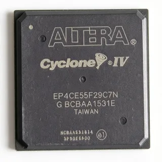
EP4CE55F29C9LN - 55K LE Cyclone IV E FPGA, 780-FBGA | Intel
MPN: EP4CE55F29C9LN ✓ Active| Qty | Unit Price | Extended |
|---|---|---|
| 1 | $34.69 | $34.69 |
| 10 | $31.21 | $312.10 |
| 100 | $27.74 | $2,774.00 |
| 250 | $25.5 | $6,375.00 |
| 500 | $23.85 | $11,925.00 |
EP4CE55F29C9LN Overview
An FPGA (Field-Programmable Gate Array) is a programmable logic device that allows engineers to implement arbitrary digital logic using configurable logic blocks (CLBs), routing interconnects, and dedicated silicon such as block RAM, DSP blocks, and PLLs. Within the broader semiconductor taxonomy, an FPGA sits below an ASIC in NRE cost but above a discrete microcontroller in logic density, and the Cyclone IV E family targets cost-sensitive, high-volume applications that previously used ASICs or ASSPs. The EP4CE55 sits in the mid-range of the family between the smaller EP4CE30 and the larger EP4CE75/EP4CE115.
Key features include 4 PLLs for clock management, up to 8 user I/O banks with LVDS support, hard memory controllers, and on-chip configuration memory. The 780-FBGA FineLine BGA package supports high I/O count with a small board footprint of approximately 29 mm × 29 mm. The 60 nm process enables typical core power well under 1 W in static and a few watts when fully utilized with moderate toggle rates.
The Cyclone IV E architecture is built around a sea-of-LABs (logic array blocks) fabric with 4-input look-up tables, fast carry chains, and adjacent M9K block RAM tiles. Each M9K block provides 9 Kbit of SRAM configurable as true dual-port or single-port RAM, FIFO, or ROM. The 374 18×18 multipliers enable cost-effective DSP functions such as FIR filters and FFT butterflies without burning logic resources, and the 4 PLLs support fractional-N synthesis, dynamic phase shifting, and spread-spectrum clocking.
Typical applications include industrial machine vision, motor control, video bridging, USB 3.0 protocol bridging, LED video walls, telecom line cards, and portable instrumentation. The combination of mid-range logic density, generous DSP and memory resources, and low static power makes the EP4CE55 well suited to mid-volume embedded designs that need parallel processing or custom high-speed I/O beyond what microcontrollers can offer.
When designing with this device, allocate sufficient decoupling on every VCCINT, VCCA, and VCCD_PLL rail. Use at least one 100 µF bulk cap per PCB plus 0.1 µF and 0.01 µF ceramics close to every ball, and follow the IBIS model for SI simulations on LVDS and DDR2/DDR3 edges.
This page synthesizes distributor pricing, drop-in Cyclone IV E alternatives from the same family, and practical design notes that go beyond the manufacturer datasheet to help engineers select and source the right FPGA variant.
Drop-in alternatives for EP4CE55F29C9LN — same package, pin-to-pin compatible. Different-package parts requiring PCB rework are excluded.
Variants in this series
Same-series models that are drop-in compatible with EP4CE55F29C9LN (same form factor and footprint) — differing in Package, Process Technology, Speed Grade, Operating Temperature, Configuration Modes.
Quick Comparison Tool — Select alternative parts for side-by-side comparison:
EP4CE55F29C8N
✅ Drop-In✓ In Stock
$285 / Unit
View Datasheet →EP4CE55F29C7N
✅ Drop-In✓ In Stock
$138 / Unit
View Datasheet →EP4CE75F29C9LN
✅ Drop-In✓ In Stock
$109.5 / Unit
View Datasheet →EP4CE115F29C9LN
✅ Drop-In📋 Reference alternative (not in catalog)
EP4CE55F29C9LN Maximum Ratings & Electrical Characteristics
| Family | Cyclone IV E |
| Logic Elements (LE) | 55,856 |
| Embedded Memory | 2,396,160 bits |
| Embedded 18x18 Multipliers | 374 |
| Logic Array Blocks (LAB) | 3,491 |
| M9K Memory Blocks | 260 |
| PLLs | 4 |
| Maximum User I/O Pins | 374 |
| Technology Node | 60 nm |
| Core Voltage (VCCINT) | 1.2 V |
| Operating Junction Temperature | 0 °C to 85 °C (commercial) |
| Package | 780-ball FBGA (F29) |
| Mounting Type | Surface Mount (BGA) |
| Lead-Free / RoHS | Yes (Pb-free terminal finish, suffix 'N') |
| Speed Grade | C9 |
EP4CE55F29C9LN 780-ball fbga (f29) Pin Configuration Guide
Pin configuration for EP4CE55F29C9LN (780-ball fbga (f29) package). This digital IC includes GPIO, communication interfaces (UART, SPI, I2C), and power pins. Refer to the manufacturer datasheet for alternate pin functions and configuration options. Essential for embedded system design and PCB layout.

No detailed pinout data available for EP4CE55F29C9LN.
Refer to the datasheet for full pin configuration.
Typical Applications
EP4CE55F29C9LN is suitable for 6 applications: Industrial Machine Vision and Image Processing, Motor Control and Industrial Drive Electronics, LED Video Wall Display Controllers, Telecom Line Cards and Protocol Bridging, Portable Test and Measurement Instrumentation, Automotive Infotainment and Driver-Assist Subsystems.
Industrial Machine Vision and Image Processing
The EP4CE55F29C9LN is well suited to multi-camera machine-vision pipelines where 374 hardware 18x18 multipliers deliver real-time FIR filtering and Sobel edge detection at 1080p60. The 2.4 Mbit of embedded SRAM (260 M9K blocks) line-buffers full-HD frames without external DDR, and the 4 PLLs generate independent pixel clocks for up to 3 MIPI-CSI or LVDS camera links via soft IP. The 780-FBGA F29 footprint exposes 374 user I/Os which is sufficient for 4-lane MIPI, GPIO for lighting strobes, and Gigabit Ethernet for result transmission. The 1.2 V VCCINT and 60 nm process keep typical vision-pipeline power under 2 W, well within industrial enclosure thermal budgets without active heatsinks.
Recommended
Motor Control and Industrial Drive Electronics
The 374 dedicated 18x18 multipliers and 4 PLLs of the EP4CE55F29C9LN enable Field-Oriented Control (FOC) loops for 3-phase PMSM and AC-induction drives, with sampling rates up to 50 kHz for high-bandwidth torque control. The 2.4 Mbit embedded memory stores sin/cos lookup tables and incremental-encoder history buffers without external SRAM, and the 8 I/O banks tolerate 2.5 V to 3.3 V signals from Hall sensors, encoders, and gate-driver feedback paths. The commercial 0-85°C junction range covers factory-floor cabinet environments, and the F29 footprint exposes 374 I/Os for parallel sigma-delta ADC sampling on the current shunt and resolver feedback channels. Hardware DSP blocks accelerate Park/Clarke transforms and space-vector PWM generation, offloading the ARM-class soft-core that often handles the supervisory state machine.
Recommended
LED Video Wall Display Controllers
The 55,856 logic elements of the EP4CE55F29C9LN drive mid-sized LED video walls up to 1024x768 with 16-bit-per-channel color depth, while the 374 hardware multipliers accelerate brightness/gamma correction and refresh-rate conversion in real time. The 2.4 Mbit embedded memory buffers scan-line data for hub-card distribution without external DDR2, and the 4 PLLs synthesize pixel clocks for the parallel LVDS outputs that fan out to multiple receiver cards. The 780-FBGA F29 footprint exposes 374 user I/Os which is enough for 24 LVDS pairs plus general-purpose hub-card control signals. The 1.2 V core and 60 nm process keep the controller below 1.5 W typical even at 60 Hz refresh, ideal for fan-less indoor cabinets where acoustic noise and reliability matter.
Recommended
Telecom Line Cards and Protocol Bridging
The EP4CE55F29C9LN is widely used in telecom equipment for protocol bridging between legacy T1/E1, HDLC, and modern Ethernet or PCIe backplanes, where 55,856 LE implement multi-channel framing, framer aggregation, and CRC engines. The 374 hardware 18x18 multipliers accelerate Reed-Solomon FEC and convolutional coding for backhaul links, and the 2.4 Mbit embedded memory queues packets between TDM and packet domains without external SSRAM. The 4 PLLs generate independent clock domains for each TDM/Ethernet port, and the 780-FBGA F29 footprint exposes enough LVDS-capable I/Os to support SGMII, GMII, and parallel TDM buses simultaneously. The commercial 0-85°C temperature range meets ATCA and NEBS-compliant central-office environments when properly thermally managed.
Recommended
Portable Test and Measurement Instrumentation
The 55,856 logic elements and 374 hardware multipliers in the EP4CE55F29C9LN enable portable oscilloscopes, logic analyzers, and protocol testers with real-time DSP at sample rates above 500 MSa/s. The 2.4 Mbit embedded memory captures trigger histories and pre-trigger samples without external DDR, and the 4 PLLs synthesize low-jitter ADC sample clocks plus trigger-arm timing for repetitive and single-shot acquisition modes. The F29 780-FBGA footprint exposes enough LVDS pairs for high-speed ADC interfaces like 14-bit 250 MSPS ADCs, while the 1.2 V VCCINT and 60 nm process deliver portable-instrument battery life in the 4-8 hour range. The commercial temperature grade is suitable for indoor lab use, and field engineers can de-rate to industrial grade parts (F29I7N) when extended temperature is required.
Recommended
Automotive Infotainment and Driver-Assist Subsystems
The EP4CE55F29C9LN (commercial grade) and its industrial-grade variant EP4CE55F29I7N are deployed in non-safety-critical automotive subsystems such as rear-seat entertainment, instrument-cluster graphics, and surround-view image stitching. The 374 hardware 18x18 multipliers accelerate surround-view warping and stitching at 30 fps for 4-camera systems, and the 2.4 Mbit embedded memory buffers multiple camera streams without external DDR. The 780-FBGA F29 footprint exposes enough LVDS pairs for 4 MIPI-CSI2 camera lanes plus an LVDS display output to the head unit. Designers must select the I-grade (EP4CE55F29I7N) or A-grade (EP4CE55F29A7N) variants for AEC-Q100-style automotive deployments since the C9LN commercial variant is restricted to 0-85°C junction temperature.
Recommended
Recommended Products Summary
Engineering reference data for EP4CE55F29C9LN — comparison, design guidance, and compliance information.
Selection Guide
Comparison with Alternatives
| Parameter | This Product | EP4CE55F29C8N | EP4CE55F29C7N | EP4CE75F29C9LN | EP4CE115F29C9LN |
|---|---|---|---|---|---|
| Package | 780-FBGA (F29) | 780-FBGA (F29) - same | 780-FBGA (F29) - same | 780-FBGA (F29) - same | 780-FBGA (F29) - same |
| Brand | Intel (Altera) | Intel (Altera) | Intel (Altera) | Intel (Altera) | Intel (Altera) |
| Logic Elements | 55,856 | 55,856 | 55,856 | 75,408 | 114,480 |
| Embedded Memory | 2,396,160 bits | 2,396,160 bits | 2,396,160 bits | 2,810,880 bits | 3,981,312 bits |
| 18x18 Multipliers | 374 | 374 | 374 | 488 | 720 |
| PLLs | 4 | 4 | 4 | 4 | 4 |
| Maximum User I/O | 374 | 374 | 374 | 426 | 426 |
| Speed Grade | C9 | C8 (faster) | C7 (fastest) | C9 | C9 |
| Junction Temperature | 0°C to 85°C | 0°C to 85°C | 0°C to 85°C | 0°C to 85°C | 0°C to 85°C |
| Process Node | 60 nm | 60 nm | 60 nm | 60 nm | 60 nm |
Key Differentiators
- Mid-range density sweet spot with 374 hardware multipliers (vs EP4CE30F29I7N)
- Pin-compatible upgrade path to EP4CE75 and EP4CE115 on same F29 footprint (vs LatticeECP3-70 (cross-vendor))
- Commercial 0-85°C temperature range at lowest cost (vs EP4CE55F29I7N (industrial grade))
Design Notes
The EP4CE55F29C9LN requires a clean 1.2 V VCCINT rail with +/-5% tolerance and a 2.5 V VCCA supply for analog PLLs. Use a dedicated switching regulator with at least 2 A peak current capability, plus 100 uF bulk + 10 uF + 0.1 uF + 0.01 uF ceramic decoupling within 5 mm of every VCCINT ball. VCCD_PLL pins (one per PLL) must each have their own pi-filter (ferrite bead + 10 uF + 0.1 uF) to isolate PLL analog domains from digital switching noise; without this decoupling the PLLs will exhibit excess jitter or fail to lock above 200 MHz.
Estimated: with theta_JA around 12 C/W on a 4-layer JEDEC test board in the F29 780-FBGA, the EP4CE55 at typical industrial toggle rate (15-20%) dissipates around 1.5 W steady-state, yielding a junction rise of approximately 18 C above ambient - well within the 85 C commercial limit. Above 30% toggle rate the power can reach 3 W (junction rise 36 C), so place thermal vias under the central ground pad array and ensure at least 4-layer PCB with continuous ground plane under the BGA. Designers targeting 100% toggle benchmark must verify with the PowerPlay Early Power Estimator before committing layout.
The 780-FBGA F29 package uses 1.0 mm ball pitch with 0.5 mm pad diameter - escape routing on inner layers requires 4 mil trace/4 mil space micro-via-in-pad (VIP) stackups. Use the Intel-provided package dimensions file in the Pin-Out Files chapter for exact ball coordinates; routing all 374 I/O plus 4 PLL clock inputs and JTAG requires 6 signal layers minimum. Matched-length routing for DDR2/DDR3 memory interfaces and LVDS pairs must follow the Cyclone IV E external memory interface handbook - LVDS data-to-clock skew must be within +/-150 ps for reliable operation at 800 Mbps.
Do not leave the MSEL[3..0] configuration mode pins floating - tie them to VCCIO8 or GND through 1 kohm resistors to select the correct configuration scheme (AS, PS, JTAG, or Fast Passive Parallel). The nCONFIG, nSTATUS, and CONF_DONE pins must each have a 10 kohm pull-up to VCCIO8 since they are open-drain. Forgetting to pull nCE low (i.e. leaving it floating) is a common cause of configuration failure; the device will not enter user mode until nCE is asserted low by the configuration controller.
Compliance Information
RoHS compliant per Altera/Intel product page. Pb-free terminal finish indicated by suffix 'N'. Halogen-free mold compound per JEDEC JS709. Commercial temperature grade only (0-85°C); for AEC-Q-style automotive deployments select I-grade (EP4CE55F29I7N) or A-grade (EP4CE55F29A7N) variants.