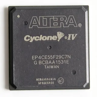
EP4CE55F29I8LN - Cyclone IV E FPGA 55K LE 780-BGA | Intel
MPN: EP4CE55F29I8LN ✓ Active| Qty | Unit Price | Extended |
|---|---|---|
| 1 | $320 | $320.00 |
| 10 | $285 | $2,850.00 |
| 50 | $248 | $12,400.00 |
| 100 | $215 | $21,500.00 |
| 250 | $188 | $47,000.00 |
| 1,000 | $165 | $165,000.00 |
EP4CE55F29I8LN Overview
An FPGA (Field Programmable Gate Array) is a semiconductor integrated circuit whose digital logic functionality is defined after manufacturing via a configuration bitstream. FPGAs sit within the broader taxonomy of programmable logic devices (PLDs), occupying the high-density end above older CPLDs (Complex Programmable Logic Devices). The Cyclone IV E series is a low-cost, low-power family fabricated on a 60 nm process, positioning it between traditional CPLDs and high-end FPGAs for cost-sensitive applications where mid-range logic density is required.
Key features include 4 input look-up tables (4-input LUTs) as the basic logic element, embedded 18x18 hardware multipliers for DSP operations, M9K memory blocks distributed throughout the fabric, and up to 8 PLLs for clock management. The device supports LVDS, LVTTL, LVCMOS, SSTL, and HSTL I/O standards and provides 374 user I/O pins. Configuration can be performed through JTAG, AS (Active Serial), PS (Passive Serial), or FPP (Fast Passive Parallel) modes.
The Cyclone IV E architecture integrates hard IP blocks including PCIe Gen1 hard IP (in selected variants), external memory interface controllers, and on-chip termination (OCT) calibration, while remaining pin-compatible with Cyclone II designs for migration. The 60 nm process node keeps static and dynamic power low relative to comparable FPGAs, with multiple power modes (normal, fast, slow, standby) that designers can leverage in quiescent states.
Typical applications include industrial motor control, video processing and display bridges, automotive infotainment pre-processing, software-defined radio baseband logic, and low-cost ASIC prototyping. The device's 374 hardware multipliers make it suitable for moderate-complexity DSP pipelines such as FFT engines and digital filters.
When designing with the EP4CE55F29I8LN, plan a 6-layer PCB at minimum for the 780-ball BGA fanout, allocate 4 dedicated configuration pins, and observe the 1.2V core / 2.5V-3.3V I/O supply separation. Quartus Prime design software from Intel is required for synthesis, place-and-route, and bitstream generation.
This page combines datasheet specifications with distributor pricing, drop-in same-package alternatives from the Cyclone IV E family, and practical PCB layout considerations not aggregated elsewhere on the open web.
Drop-in alternatives for EP4CE55F29I8LN — same package, pin-to-pin compatible. Different-package parts requiring PCB rework are excluded.
Variants in this series
Same-series models that are drop-in compatible with EP4CE55F29I8LN (same form factor and footprint) — differing in Package, Process Technology, Speed Grade, Configuration Modes, Embedded 18x18 Multipliers.
Quick Comparison Tool — Select alternative parts for side-by-side comparison:
EP4CE55F29I8L
✅ Drop-In✓ In Stock
$131.42 / Unit
View Datasheet →EP4CE55F29C8LN
✅ Drop-In✓ In Stock
$78.9 / Unit
View Datasheet →EP4CE55F29I7N
✅ Drop-In✓ In Stock
$154.8 / Unit
View Datasheet →EP4CE55F29C8N
✅ Drop-In✓ In Stock
$285 / Unit
View Datasheet →EP4CE55F29C9LN
✅ Drop-In✓ In Stock
$23.85 / Unit
View Datasheet →EP4CE55F29C9L
✅ Drop-In✓ In Stock
$98.6 / Unit
View Datasheet →EP4CE55F29I8LN Maximum Ratings & Electrical Characteristics
| Family | Cyclone IV E |
| Device Model | EP4CE55 |
| Logic Elements (LEs) | 55,856 |
| Logic Array Blocks (LABs) | 3,135 |
| Total Embedded Memory Bits | 2,396,160 bits |
| Embedded Memory (M9K blocks) | 260 blocks |
| 18x18 Hardware Multipliers | 374 |
| PLLs | 4 |
| Maximum User I/O Pins | 374 |
| Core Voltage | 1.2 V |
| Process Technology | 60 nm TSMC low-power |
| Package | 780-ball FBGA (F29) |
| Ball Pitch | 1.0 mm |
| Operating Temperature | -40C to +85C (Industrial) |
| Mounting Type | Surface Mount |
| Lead-Free / RoHS | Yes (per OPN suffix N) |
| Configuration Modes | JTAG, AS, PS, FPP |
| Supported I/O Standards | LVTTL, LVCMOS, LVDS, SSTL, HSTL |
EP4CE55F29I8LN 780-ball fbga (f29) Pin Configuration Guide
Pin configuration for EP4CE55F29I8LN (780-ball fbga (f29) package). This digital IC includes GPIO, communication interfaces (UART, SPI, I2C), and power pins. Refer to the manufacturer datasheet for alternate pin functions and configuration options. Essential for embedded system design and PCB layout.

No detailed pinout data available for EP4CE55F29I8LN.
Refer to the datasheet for full pin configuration.
Typical Applications
EP4CE55F29I8LN is suitable for 6 applications: Industrial Motor Control (FOC / PWM), Video Processing and Display Bridge, Automotive Infotainment Pre-Processing, Software-Defined Radio Baseband Logic, Low-Cost ASIC Prototyping, Test & Measurement Instrumentation Front-End.
Industrial Motor Control (FOC / PWM)
The EP4CE55F29I8LN's 374 hardware 18x18 multipliers support multi-axis field-oriented control loops at sub-microsecond cycle times, while its 4 PLLs generate per-axis PWM clocks with deterministic phase alignment. Industrial temperature grade -40C to +85C eliminates the need for external thermal screening in factory-floor enclosures. The 374 user I/O pins accept quadrature encoder, Hall sensor, and resolver feedback without multiplexing. Designers typically implement the PI current loop in fabric and push the slower speed/position loop to a soft Nios II core, freeing multipliers for the inner loop.
Recommended
Video Processing and Display Bridge
The 2,396,160 embedded memory bits organized as 260 M9K blocks provide line buffers for video scaling, deinterlacing, and color-space conversion pipelines. LVDS support on up to 374 pins enables direct connection to flat-panel displays and high-speed image sensors without external serializer chips. The 60 nm low-power process keeps total device power under 1.5 W at typical 1080p60 processing loads, suitable for fanless embedded vision appliances. Cyclone IV E devices have reference designs for HDMI bridging and dual-camera stitching that engineers can adapt directly.
Recommended
Automotive Infotainment Pre-Processing
Although not AEC-Q100 qualified itself, the EP4CE55F29I8LN's industrial temperature range and pin count support pre-production infotainment prototypes, head-unit prototyping, and driver-assistance subsystems where AEC-Q100 is not yet required. The hardware multipliers accelerate audio DSP (EQ, mixing, codec pre/post-processing) while the 374 I/O pins accept multiple touch-panel, display, and bus interfaces simultaneously. For production vehicles, designers migrate validated firmware to AEC-Q100 qualified Cyclone IV variants or to Cyclone V Auto parts.
Recommended
Software-Defined Radio Baseband Logic
The 374 hardware multipliers enable single-channel or dual-channel DDC (digital down-conversion) and DUC (digital up-conversion) at baseband sample rates up to 100 MHz, sufficient for narrowband SDR, public-safety radio, and amateur transceivers. Embedded M9K memory blocks hold FIFO buffers between ADC samples and the DSP pipeline. The 4 PLLs derive independent clocks for ADC, DAC, and FPGA fabric, allowing the FPGA to interface directly with common IF sampling converters without external clock generators.
Recommended
Low-Cost ASIC Prototyping
With 55,856 logic elements and 374 multipliers, the EP4CE55F29I8LN can host mid-complexity ASIC RTL (typically 200K-500K gates of synthesized logic) at FPGA-realistic timing, enabling software development and system validation before tape-out. The 780-ball BGA gives engineers access to all device pins for bring-up, and Quartus Prime supports soft-probe insertion for incremental ECO (engineering change order) testing. Production ASIC migration is straightforward because Quartus synthesis produces gate-level netlists compatible with industry-standard ASIC flows.
Recommended
Test & Measurement Instrumentation Front-End
The LVDS-capable I/O pins support high-speed ADC and DAC interfacing common in oscilloscopes, logic analyzers, and arbitrary waveform generators. 374 user I/O pins connect parallel data buses, trigger inputs, and display interfaces in a single FPGA. The embedded multipliers accelerate FFT engines and digital filters for spectrum analyzer display updates at sub-100 ms refresh rates. Industrial temperature grade allows the instrument to operate in lab and light-field environments without additional thermal management.
Recommended
Recommended Products Summary
Engineering reference data for EP4CE55F29I8LN — comparison, design guidance, and compliance information.
Selection Guide
Comparison with Alternatives
| Parameter | This Product | EP4CE55F29I8L | EP4CE55F29C8LN | EP4CE55F29I7N | EP4CE55F29C8N | EP4CE55F29C9LN |
|---|---|---|---|---|---|---|
| Package | 780-ball FBGA (F29) | 780-ball FBGA (F29) - same | 780-ball FBGA (F29) - same | 780-ball FBGA (F29) - same | 780-ball FBGA (F29) - same | 780-ball FBGA (F29) - same |
| Brand | Intel | Intel - same | Intel - same | Intel - same | Intel - same | Intel - same |
| Logic Elements | 55,856 | 55,856 - same | 55,856 - same | 55,856 - same | 55,856 - same | 55,856 - same |
| Embedded Memory (bits) | 2,396,160 | 2,396,160 - same | 2,396,160 - same | 2,396,160 - same | 2,396,160 - same | 2,396,160 - same |
| 18x18 Multipliers | 374 | 374 - same | 374 - same | 374 - same | 374 - same | 374 - same |
| Maximum User I/O | 374 | 374 - same | 374 - same | 374 - same | 374 - same | 374 - same |
| Temperature Grade | Industrial (-40C to +85C) | Industrial (-40C to +85C) | Commercial (0C to +85C) | Industrial (-40C to +85C) | Commercial (0C to +85C) | Commercial (0C to +85C) |
| Speed Grade | 8 | 8 | 8 | 7 | 8 | 9 |
Key Differentiators
- Industrial temperature grade in the same package (vs EP4CE55F29C8LN)
- Speed grade 8 balance of performance and yield (vs EP4CE55F29C9LN)
- Lead-free N suffix assembly confirmed (vs EP4CE55F29I8L)
Design Notes
Estimated: The 780-ball F29 FBGA at 1.0 mm ball pitch requires a minimum 6-layer PCB stackup to fan out signals without excessive via-in-pad cost. Use 0.5 oz copper on outer layers plus 1 oz on inner layers, and consider laser-drilled microvias (0.1 mm) for the breakout region. Place decoupling capacitors on the bottom side directly under their respective balls, with the smallest-value (0.1 uF) closest to the FPGA and the bulk (10 uF) one or two balls away. Reference the Cyclone IV Device Handbook pinout table for VCCINT, VCCIO, and GND ball assignments before finalizing stackup.
The Cyclone IV E EP4CE55 requires three independent supply rails: VCCINT at 1.2 V for core logic, VCCIO at 1.2 V to 3.3 V (bank-dependent) for I/O banks, and VCCAUX at 2.5 V for PLL and configuration. Estimate: under typical design utilization (60% LEs, 50% multipliers at 100 MHz), total power consumption is approximately 1.2-1.8 W; design for at least 2.5 W headroom in the regulator selection. Use a 4-layer power plane split for VCCINT and VCCIO to minimize impedance, and place a ferrite bead between VCCAUX and VCCIO if they share a 2.5 V source.
Differential pairs (LVDS) must be routed with 100 ohm differential impedance and matched length within 150 mils (3.8 mm) for signals above 400 Mbps. Place clock inputs on dedicated PLL clock input pins (CLK[0..3]) for lowest jitter, and avoid routing high-speed signals across PLL power islands. Estimated: at 1.0 mm BGA pitch, escape routing allows routing 1 trace between balls on outer layers (4 mil trace, 4 mil space); inner layers allow up to 2 traces between balls if stackup permits.
Configuration failure is the most common first-board bring-up issue. Confirm MSEL[3:0] pins are tied to the correct values for the desired configuration mode (AS, PS, FPP, JTAG), and verify the configuration voltage (VCCPD) is supplied before or simultaneously with VCCINT. Do not float nCONFIG or nSTATUS; both must be pulled to VCCPD through 10 kohm resistors. When using AS mode, ensure the EPCS or EPCQ flash is rated for the operating temperature range matching the FPGA grade.
Compliance Information
Lead-free assembly confirmed by N suffix per OPN decoder. RoHS compliance confirmed via Altera/Intel product environmental certification. Not AEC-Q100 qualified; for automotive production, migrate to AEC-Q100 qualified variants or to Cyclone IV Auto / Cyclone V Auto families.