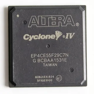
EP4CE40F29C6N - Cyclone IV E FPGA 39.6K LE | Intel | 780-BGA
MPN: EP4CE40F29C6N ✓ Active| Qty | Unit Price | Extended |
|---|---|---|
| 1 | $129.19 | $129.19 |
| 10 | $116.27 | $1,162.70 |
| 100 | $103.35 | $10,335.00 |
| 500 | $90.43 | $45,215.00 |
| 1,000 | $77.51 | $77,510.00 |
EP4CE40F29C6N Overview
What is an FPGA? A Field Programmable Gate Array is a digital semiconductor containing an array of configurable logic blocks (CLBs), programmable interconnect, and dedicated hard IP such as memory blocks, DSP blocks, PLLs, and SERDES. FPGAs sit in the programmable-logic tier of the broader digital-semiconductor hierarchy: ASIC < FPGA < programmable SoC < microprocessor. The Cyclone IV E family was engineered for cost-sensitive, high-volume applications that previously used ASICs or CPLDs.
Key features of the EP4CE40F29C6N include 39,600 logic elements arranged into 4-input adaptive logic modules (ALMs), 4 M9K embedded memory blocks (113 blocks total) totaling 1,161,216 RAM bits, 66 18x18 hardware multipliers, four general-purpose PLLs, and 532 maximum user I/Os. The 780-BGA (F29) package provides the highest I/O count and largest pin pitch of the EP4CE40 family, suitable for high-density board designs.
Architecturally, the Cyclone IV E device uses a 1.2 V core supplied by an on-die linear regulator. Configuration is via serial (AS) flash, JTAG, or passive serial. Static power consumption is among the lowest in its class, and the device supports hot-socketing and octal configuration modes. The 60 nm TSMC process allows operation down to 1.0 V core with internal regulation.
Typical applications include industrial motor control and machine vision, automotive infotainment prototypes, video processing and display controllers, communications line cards, software-defined radio front-ends, and ASIC prototyping. The wide logic and DSP capacity also make it useful for embedded data acquisition and DSP co-processing.
Designers should plan FPGA power sequencing with the 1.2 V core supply ramped first and the I/O banks following, follow Altera's recommended decoupling scheme, and use the Quartus II/Prime toolchain for place-and-route.
This page consolidates Cyclone IV E pricing, drop-in FPGA alternatives, and design notes that complement the official datasheet.
Drop-in alternatives for EP4CE40F29C6N — same package, pin-to-pin compatible. Different-package parts requiring PCB rework are excluded.
Variants in this series
Same-series models that are drop-in compatible with EP4CE40F29C6N (same form factor and footprint) — differing in Package, Operating Temperature, Speed Grade, Process Technology, Configuration Modes.
Quick Comparison Tool — Select alternative parts for side-by-side comparison:
EP4CE40F29I7N
✅ Drop-In✓ In Stock
$124 / Unit
View Datasheet →EP4CE40F29C7N
✅ Drop-In✓ In Stock
$55.85 / Unit
View Datasheet →EP4CE40F29C8N
✅ Drop-In✓ In Stock
$104.6 / Unit
View Datasheet →EP4CE30F29C7N
✅ Drop-In📋 Reference alternative (not in catalog)
EP4CE55F29C6N
✅ Drop-In✓ In Stock
$49.95 / Unit
View Datasheet →EP4CE40F29C6N Maximum Ratings & Electrical Characteristics
| Family | Cyclone IV E |
| Logic Elements | 39,600 |
| Embedded Memory (bits) | 1,161,216 |
| Embedded Memory Blocks | 113 M9K blocks |
| 18x18 Hardware Multipliers | 66 |
| PLLs | 4 general-purpose |
| Maximum User I/Os | 532 |
| Package | 780-ball FBGA (F29) |
| Process Node | 60 nm |
| Core Voltage | 1.2 V (internal regulated) |
| Operating Temperature | 0°C to +85°C (commercial) |
| Speed Grade | 6 |
| Configuration Modes | Serial, JTAG, Passive Serial, AS |
| Mounting Type | Surface Mount |
| MSL Level | 3 |
| RoHS Status | Compliant |
EP4CE40F29C6N 780-ball fbga (f29) Pin Configuration Guide
Pin configuration for EP4CE40F29C6N (780-ball fbga (f29) package). This digital IC includes GPIO, communication interfaces (UART, SPI, I2C), and power pins. Refer to the manufacturer datasheet for alternate pin functions and configuration options. Essential for embedded system design and PCB layout.

No detailed pinout data available for EP4CE40F29C6N.
Refer to the datasheet for full pin configuration.
Typical Applications
EP4CE40F29C6N is suitable for 7 applications: Industrial Motor Control, Machine Vision and Video Processing, Software-Defined Radio Front-End, ASIC Prototyping, Communications Line Cards, Embedded Data Acquisition and DSP Co-Processing, Automotive Infotainment Prototyping.
Industrial Motor Control
The EP4CE40F29C6N is well suited to industrial motor-control applications where multiple encoder interfaces, PWM generators, and PID control loops must run deterministically. Its 66 dedicated 18x18 hardware multipliers enable real-time field-oriented control (FOC) algorithms without taxing the fabric, while 113 M9K memory blocks (1.16 Mbit) hold commutation tables and current-loop state. The 532 user I/Os of the F29 package accept many simultaneous quadrature-encoder and resolver channels, and the commercial 0–85°C grade covers most factory-floor enclosures.
Recommended
Machine Vision and Video Processing
With 39,600 logic elements and 66 hardware multipliers, the EP4CE40F29C6N can perform real-time pixel processing, color-space conversion, and edge detection for industrial camera pipelines. The 1.16 Mbit of embedded memory buffers line-scan data at typical Camera Link rates, while 532 I/Os let designers parallel-route multiple MIPI-CSI2 or LVDS sensor lanes directly into the F29 BGA. Quartus IP for VIP and Video Bridging accelerates integration with external image sensors.
Recommended
Software-Defined Radio Front-End
The EP4CE40F29C6N's 66 18x18 hardware multipliers and four general-purpose PLLs make it a flexible baseband processor for software-defined radio (SDR) front-ends below 100 MHz bandwidth. Designers implement digital down-conversion, filtering, and demodulation in fabric while the PLLs synthesize the local-oscillator and sampling clocks. The large F29 BGA exposes enough LVDS pairs to interface directly with ADC eval boards, and the 1.16 Mbit embedded RAM holds sample buffers for short bursts.
Recommended
ASIC Prototyping
The 39,600 logic elements, 1.16 Mbit memory, and 66 multipliers of the EP4CE40F29C6N make it a cost-effective vehicle for prototyping mid-complexity ASICs. Designers map RTL from the target ASIC, run real-world firmware, and validate I/O behavior before committing to silicon. The F29 780-BGA exposes enough user I/Os to mirror most ASIC signal pads, and the same die scales within the Cyclone IV E family (EP4CE55, EP4CE75, EP4CE115) for design exploration.
Recommended
Communications Line Cards
Telecom line-card designs leverage the EP4CE40F29C6N for glue logic, TDM switching, and SERDES-adjacent protocol conversion where deterministic latency matters. The four PLLs synthesize independent clock domains for backplane, framer, and processor interfaces, while 532 I/Os of the F29 package accommodate parallel TDM buses, SPI/parallel peripheral buses, and management interfaces. Quartus IP for UTOPIA / Serial RapidIO eases integration with legacy line-card ASICs.
Recommended
Embedded Data Acquisition and DSP Co-Processing
The 66 hardware multipliers of the EP4CE40F29C6N deliver up to ~250 MHz of 18x18 multiply-accumulate throughput, ideal as a DSP co-processor beside a microcontroller or ARM host. The 1.16 Mbit of embedded memory stores FIR/IIR coefficient banks and circular sample buffers, while the 532 I/Os expose parallel ADC/DAC buses and SPI/I2C control. The Cyclone IV E family is supported by the Quartus II / Quartus Prime toolchain with mature DSP Builder integration.
Recommended
Automotive Infotainment Prototyping
Designers prototype CAN/LIN bridging, LVDS display pipelines, and audio-routing fabrics on the EP4CE40F29C6N before committing to an automotive-grade ASIC. The 39,600 logic elements handle multiple display layers and audio mixers simultaneously, while 113 M9K memory blocks provide frame-buffer storage. Although the EP4CE40F29C6N is commercial 0–85°C, the same die is offered in industrial (EP4CE40F29I7N) for cabin environments and validated through Intel's automotive FPGA program.
Recommended
Recommended Products Summary
Engineering reference data for EP4CE40F29C6N — comparison, design guidance, and compliance information.
Selection Guide
Comparison with Alternatives
| Parameter | This Product | EP4CE40F29I7N | EP4CE40F29C7N | EP4CE40F29C8N | EP4CE30F29C7N | EP4CE55F29C6N |
|---|---|---|---|---|---|---|
| Package | 780-ball FBGA (F29) | 780-ball FBGA (F29) - same | 780-ball FBGA (F29) - same | 780-ball FBGA (F29) - same | 780-ball FBGA (F29) - same | 780-ball FBGA (F29) - same |
| Brand | Intel (formerly Altera) | Intel - same | Intel - same | Intel - same | Intel - same | Intel - same |
| Logic Elements | 39,600 | 39,600 (same die) | 39,600 (same die) | 39,600 (same die) | 28,848 (-27%) | 55,856 (+41%) |
| Embedded Memory (bits) | 1,161,216 | 1,161,216 | 1,161,216 | 1,161,216 | 608,256 (-48%) | 2,343,936 (+102%) |
| 18x18 Multipliers | 66 | 66 | 66 | 66 | 66 | 156 |
| User I/Os | 532 | 532 | 532 | 532 | 532 | 532 |
| Speed Grade | 6 | 7 | 7 | 8 (fastest) | 7 | 6 |
| Temperature Grade | Commercial 0C to +85C | Industrial -40C to +100C | Commercial 0C to +85C | Commercial 0C to +85C | Commercial 0C to +85C | Commercial 0C to +85C |
Key Differentiators
- Same F29 780-ball footprint as the rest of the EP4CE40/30/55 family (vs EP4CE40F23C6N)
- Mid-density Cyclone IV E with 1.16 Mbit embedded memory (vs EP4CE30F29C7N)
- Speed grade 6 with Quartus Prime support (vs EP4CE40F29C8N)
Design Notes
Cyclone IV E devices derive their 1.2 V core from an internal linear regulator powered by VCCINT. The regulator requires a 0.1 uF decoupling capacitor as close as physically possible to the VCCINT pins, plus a bulk 4.7 uF–22 uF tantalum or ceramic capacitor. Estimated: VCCINT current for the EP4CE40F29C6N at full utilization is roughly 500–800 mA; design the 3.3 V VCCIO supply with at least 1 A headroom if many I/O banks toggle simultaneously.
The 780-ball F29 FBGA uses a 1.0 mm ball pitch. Route all signals on inner layers with microvias (stacked or staggered) and escape the perimeter balls through the top layer. Use a 4–6 layer stack-up with continuous GND planes beneath the package for thermal spreading and return-path integrity. Follow Intel/Altera's recommended land pattern and via-in-pad guidelines for BGA fan-out.
Do not hot-plug JTAG or configuration signals without series resistors; the Cyclone IV E configuration pins are not 5 V-tolerant unless documented. Always program the configuration mode pins MSEL[3..0] correctly for the selected mode (AS, PS, JTAG, FPP) - misprogramming causes the device to fail configuration. Verify the AS configuration clock (DCLK) does not exceed 100 MHz and that the serial flash is rated for the read mode selected.
Estimated: at 100% resource utilization with 66 multipliers at 250 MHz, the EP4CE40F29C6N junction temperature can rise 15–25°C above ambient on a 4-layer JEDEC test board. For enclosed industrial enclosures, derate to 70% utilization or add a small heatsink / thermal via array under the package thermal pad. Use the Quartus PowerPlay early power estimator before PCB commit.
Compliance Information
RoHS and lead-free per Intel/Altera Cyclone IV E product page. AEC-Q100 not applicable (FPGA, not automotive-grade IC). Halogen-free status not explicitly stated in the provided data.