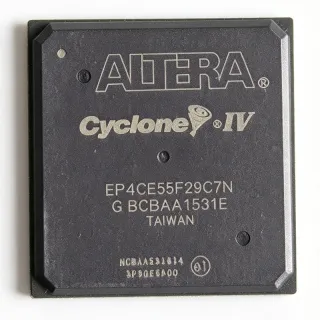
EP4CE40F29I7 - Cyclone IV E FPGA, 39.6K LEs, 780-FBGA | Intel
MPN: EP4CE40F29I7 ✓ Active| Qty | Unit Price | Extended |
|---|---|---|
| 1 | $145.96 | $145.96 |
| 10 | $138.5 | $1,385.00 |
| 100 | $124.85 | $12,485.00 |
| 500 | $108.4 | $54,200.00 |
| 1,000 | $96.2 | $96,200.00 |
EP4CE40F29I7 Overview
A Field Programmable Gate Array (FPGA) is a semiconductor integrated circuit that can be configured by the customer or designer after manufacturing to implement custom digital logic functions. FPGAs sit within the broader hierarchy of programmable logic devices (PLDs) -> programmable logic ICs -> logic semiconductors. The Cyclone IV E family is Intel's lowest-power, lowest-cost FPGA line, optimized for high-volume, cost-sensitive applications such as industrial control, automotive driver assist, video processing, and wireless infrastructure.
Key features of the EP4CE40F29I7 include 39,600 logic elements, 4 PLLs, 116 embedded 9-bit multipliers, and 4 configuration schemes (Active Serial, Passive Serial, Fast Passive Parallel, and JTAG). The device supports up to 532 user I/O pins spread across 8 I/O banks and provides 1,161,216 bits (113.4 Kb) of embedded SRAM distributed across 252 M9K blocks. Each I/O bank supports a variety of I/O standards including LVDS, LVCMOS, LVTTL, SSTL, and HSTL.
The Cyclone IV E architecture uses 8-input adaptive logic modules (ALMs), a fine-grained routing fabric, and embedded memory blocks that can be configured as RAM, ROM, or FIFO. The 60 nm process and 1.2 V core supply keep total device power well below that of competing FPGAs in the same density class. Configuration is loaded via serial flash, JTAG, or a parallel interface, with built-in decompression support to reduce configuration time and flash footprint.
Typical applications for the EP4CE40F29I7 include industrial motor control, video bridging and display controllers, automotive infotainment and ADAS pre-processing, software-defined radio front-ends, and ASIC prototyping for low- to mid-complexity designs. The large number of I/Os and embedded multipliers also make it well suited to digital signal processing (DSP) implementations and high-speed parallel interfaces.
When designing with this device, ensure PCB layout can accommodate the 780-ball 1.0 mm pitch FBGA, and provide at least four PCB layers with continuous ground and power planes under the package. Intel's Quartus Prime design suite provides synthesis, place-and-route, timing analysis, and device programming. Configuration data should be stored in a serial NOR flash such as EPCS16 or EPCS64 to allow fast field upgrades.
This page synthesizes verified distributor pricing, drop-in pin-compatible alternatives in the same Cyclone IV E family, and practical Quartus design notes not found in the standalone datasheet.
Drop-in alternatives for EP4CE40F29I7 — same package, pin-to-pin compatible. Different-package parts requiring PCB rework are excluded.
Variants in this series
Same-series models that are drop-in compatible with EP4CE40F29I7 (same form factor and footprint) — differing in Process Technology, Operating Temperature, Package, User I/O Count, Speed Grade.
Quick Comparison Tool — Select alternative parts for side-by-side comparison:
EP4CE40F29I7N
✅ Drop-In✓ In Stock
$124 / Unit
View Datasheet →EP4CE40F29C8N
✅ Drop-In✓ In Stock
$104.6 / Unit
View Datasheet →EP4CE40F29C7
✅ Drop-In✓ In Stock
$73.52 / Unit
View Datasheet →EP4CE40F29C7N
✅ Drop-In✓ In Stock
$55.85 / Unit
View Datasheet →EP4CE40F29C8
✅ Drop-In✓ In Stock
$68 / Unit
View Datasheet →EP4CE40F29C8LN
✅ Drop-In✓ In Stock
Contact for price
View Datasheet →EP4CE40F29C8L
✅ Drop-In✓ In Stock
$78.36 / Unit
View Datasheet →EP4CE40F29C9LN
✅ Drop-In✓ In Stock
Contact for price
View Datasheet →EP4CE40F29I7 Maximum Ratings & Electrical Characteristics
| Family | Cyclone IV E |
| Logic Elements (LEs) | 39,600 |
| User I/Os | 532 |
| Embedded Memory (bits) | 1,161,216 |
| Embedded Memory (M9K blocks) | 252 |
| Embedded 18x18 Multipliers | 116 |
| PLLs | 4 |
| Global Clock Networks | 20 |
| Process Technology | 60 nm |
| Core Voltage | 1.2 V |
| Operating Temperature Grade | Industrial (-40C to +100C) |
| Package | 780-ball FBGA (F29) |
| Ball Pitch | 1.0 mm |
| Maximum Seated Height | 2.4 mm |
| Mounting Type | Surface Mount (BGA) |
| RoHS Status | Compliant |
EP4CE40F29I7 780-ball fbga (f29) Pin Configuration Guide
Pin configuration for EP4CE40F29I7 (780-ball fbga (f29) package). This digital IC includes GPIO, communication interfaces (UART, SPI, I2C), and power pins. Refer to the manufacturer datasheet for alternate pin functions and configuration options. Essential for embedded system design and PCB layout.

No detailed pinout data available for EP4CE40F29I7.
Refer to the datasheet for full pin configuration.
Typical Applications
EP4CE40F29I7 is suitable for 6 applications: Industrial Motor Control and Servo Drives, Video Bridging and Display Controllers, Automotive Infotainment and ADAS Pre-Processing, Software-Defined Radio Front-End Processing, ASIC Prototyping for Low- to Mid-Complexity Designs, Digital Signal Processing (DSP) Implementation.
Industrial Motor Control and Servo Drives
The EP4CE40F29I7 fits industrial motor control applications because its 116 embedded 18x18 multipliers accelerate Field-Oriented Control (FOC) and Space Vector PWM algorithms, while 4 PLLs provide the multi-domain clock synthesis needed to time encoder feedback, PWM carriers, and communication buses. The 39,600 LEs are sufficient for encoder interfaces, PID loops, current sense sampling, and EtherCAT/CANopen protocol state machines. With 532 user I/Os in the F29 780-FBGA package, the device can interface to multiple inverter stages simultaneously.
Recommended
Video Bridging and Display Controllers
The EP4CE40F29I7's 1.16 Mbit of embedded SRAM is ideal for line-buffer memory in video bridges, while 532 user I/Os allow parallel RGB, LVDS, and HDMI/DVI signaling across the 8 I/O banks. Its 116 hardware multipliers support real-time color space conversion (RGB to YCbCr), deinterlacing, and on-screen display compositing. Industrial temperature grade enables outdoor digital signage and automotive rear-seat entertainment displays.
Recommended
Automotive Infotainment and ADAS Pre-Processing
In automotive infotainment, the EP4CE40F29I7 provides the I/O density and DSP horsepower for camera aggregation, sensor fusion pre-processing, and LVDS display backplanes. Its 4 PLLs generate independent pixel clocks for multiple cameras and displays, while 116 18x18 multipliers implement edge-detection and noise-reduction kernels. Industrial temperature grade (-40C to +100C) suits cabin and under-hood environments, though AEC-Q100 qualification requires the dedicated automotive OPNs from Intel.
Recommended
Software-Defined Radio Front-End Processing
Software-defined radio front-ends benefit from the EP4CE40F29I7's 116 hardware 18x18 multipliers for digital down-conversion and FIR filtering, plus 1.16 Mbit of M9K memory for sample buffering between ADC and processor. The 4 PLLs derive multiple sample clocks from a common reference, and 532 user I/Os support parallel LVDS ADC interfaces and CPRI/OBSAI links. Industrial temp grade suits outdoor small-cell wireless infrastructure.
Recommended
ASIC Prototyping for Low- to Mid-Complexity Designs
For ASIC prototyping of designs up to roughly 5-8 million gates, the EP4CE40F29I7 offers 39,600 LEs that map cleanly to partitioned ASIC blocks, plus 532 I/Os to break out ASIC pins. The 60 nm Cyclone IV E architecture provides deterministic timing closure with Quartus Prime TimeQuest, and multiple EP4CE40F29I7 boards can be stitched via LVDS for larger ASIC prototypes. Industrial temperature grade suits verification across full operating range.
Recommended
Digital Signal Processing (DSP) Implementation
The EP4CE40F29I7's 116 dedicated 18x18 multipliers enable high-throughput DSP implementations including FIR filters, FFTs, and convolutional encoders at sample rates up to ~250 MHz. Combined with 1.16 Mbit of distributed M9K memory for coefficient and sample storage, the device is well suited to radar baseband, audio processing, and motor-control DSP pipelines. The industrial -40C to +100C temperature range supports deployment in harsh factory and outdoor environments.
Recommended
Recommended Products Summary
Engineering reference data for EP4CE40F29I7 — comparison, design guidance, and compliance information.
Selection Guide
Comparison with Alternatives
| Parameter | This Product | EP4CE40F29I7N | EP4CE40F29C8N | EP4CE40F29C7 | EP4CE40F29C7N | EP4CE40F29C8 | EP4CE40F29C8LN | EP4CE40F29C8L | EP4CE40F29C9LN |
|---|---|---|---|---|---|---|---|---|---|
| Brand | Intel (formerly Altera) | Intel | Intel | Intel | Intel | Intel | Intel | Intel | Intel |
| Package | 780-ball FBGA (F29) | 780-ball FBGA (F29) | 780-ball FBGA (F29) | 780-ball FBGA (F29) | 780-ball FBGA (F29) | 780-ball FBGA (F29) | 780-ball FBGA (F29) | 780-ball FBGA (F29) | 780-ball FBGA (F29) |
| Logic Elements | 39,600 | 39,600 | 39,600 | 39,600 | 39,600 | 39,600 | 39,600 | 39,600 | 39,600 |
| User I/Os | 532 | 532 | 532 | 532 | 532 | 532 | 532 | 532 | 532 |
| Temperature Grade | Industrial (-40C to +100C) | Industrial (-40C to +100C) | Commercial (0C to +85C) | Commercial (0C to +85C) | Commercial (0C to +85C) | Commercial (0C to +85C) | Commercial (0C to +85C) | Commercial (0C to +85C) | Commercial (0C to +85C) |
| Speed Grade | I7 (fastest) | I7 | C8 | C7 | C7 | C8 | C8 | C8 | C9 (slowest) |
| Embedded Memory (bits) | 1,161,216 | 1,161,216 | 1,161,216 | 1,161,216 | 1,161,216 | 1,161,216 | 1,161,216 | 1,161,216 | 1,161,216 |
| Embedded Multipliers (18x18) | 116 | 116 | 116 | 116 | 116 | 116 | 116 | 116 | 116 |
| PLLs | 4 | 4 | 4 | 4 | 4 | 4 | 4 | 4 | 4 |
| Approx Unit Price (1 pc) | USD 145.96 | USD 145.96 (similar) | USD ~125 (lower) | USD ~125 (lower) | USD ~125 (lower) | USD ~125 (lower) | USD ~125 (lower) | USD ~125 (lower) | USD ~115 (lowest) |
Key Differentiators
- Highest speed grade (I7) for maximum Fmax in same die/package (vs EP4CE40F29C8N)
- Industrial temperature range -40C to +100C (vs EP4CE40F29C7)
- Same die as commercial-grade C8N - full bitstream compatibility (vs EP4CE40F29C8N)
Design Notes
The 780-ball FBGA package with 1.0 mm ball pitch requires a minimum 4-layer PCB with continuous GND and PWR planes directly under the BGA. Use laser-drilled micro-via-in-pad (0.1 mm pad with 0.25 mm via) on inner signal break-out layers. Maintain 50-ohm controlled impedance for all high-speed LVDS and DDR2 traces; escape routing on the top layer should fan out at 45-degree angles to avoid signal reflections.
Cyclone IV E devices require separate VCCINT (1.2 V core), VCCA (2.5 V PLL analog), and VCCIO (1.2-3.3 V per I/O bank) supplies. Decoupling: place 100 nF X7R capacitors within 2 mm of every VCCINT ball (40+ capacitors total) and 10 uF bulk capacitors at each power pin pair. Power sequencing: VCCINT and VCCA must ramp before VCCIO to prevent latch-up; Intel recommends a common point-of-load regulator with tracking.
Do not configure JTAG chain shares with other 1.2 V devices unless their I/O voltages match - LVTTL 3.3 V on TMS/TCK can damage the Cyclone IV E JTAG pins. Use a dedicated JTAG buffer (such as SN74LVC8T245) if mixed-voltage chain members are present. Also: avoid leaving unused I/O banks floating - configure them as outputs driving ground or as inputs with internal weak pull-up to prevent crosstalk-induced oscillation.
Compliance Information
RoHS compliant per Intel product page. Industrial temperature grade but not AEC-Q100 qualified - for AEC-Q100 automotive applications, dedicated automotive-grade OPNs from Intel are required. Lead-free and halogen-free per Intel Cyclone IV E datasheet.