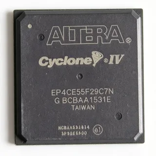
EP4CE55F29C9L - Cyclone IV E 55K LEs FPGA | Intel | 780-FBGA
MPN: EP4CE55F29C9L ✓ Active| Qty | Unit Price | Extended |
|---|---|---|
| 1 | $151.02 | $151.02 |
| 10 | $138.5 | $1,385.00 |
| 100 | $125.4 | $12,540.00 |
| 500 | $112.8 | $56,400.00 |
| 1,000 | $98.6 | $98,600.00 |
EP4CE55F29C9L Overview
An FPGA (field-programmable gate array) is a semiconductor IC containing an array of configurable logic blocks (CLBs), programmable interconnects, and dedicated hardware resources (block RAM, DSP blocks, PLLs, transceivers) that engineers can program post-fabrication to implement arbitrary digital logic. FPGAs sit between general-purpose microcontrollers and ASICs in the flexibility/performance/cost hierarchy: more flexible than ASICs, faster and more parallel than MCUs, and cheaper in low volumes than custom silicon. Cyclone IV E devices specifically belong to the low-cost, low-power FPGA segment, making them suitable for replacing discrete logic, glue logic, and small-to-medium state machines.
The EP4CE55F29C9L provides up to 154 embedded 18x18 multipliers for DSP, 4 general-purpose PLLs, and supports LVDS, LVCMOS, SSTL, and HSTL I/O standards. Cyclone IV E parts include a hard PCIe Gen1 x4 PHY block and dedicated DDR/DDR2 SDRAM controllers. Configuration is supported via JTAG, active serial (AS), passive serial (PS), and fast passive parallel (FPP) modes. The 'F29' speed grade combined with the 'C9' commercial temperature rating (0C to +85C) yields a balanced cost/performance positioning for typical commercial designs.
Typical applications include industrial motor control and machine vision, broadcast video processing and switching, telecommunications baseband preprocessing, and automotive infotainment prototypes. The large 780-ball BGA footprint supports designs requiring maximum I/O count and signal integrity for parallel bus architectures.
When designing with this device, allocate sufficient PCB area for the 29x29 mm BGA land pattern and follow Intel's power-rail decoupling guidance. Configuration mode selection requires correct MSEL pin strapping before power-up; misconfiguration can prevent the device from entering user mode. Use Intel Quartus Prime software for synthesis, place-and-route, and timing closure.
This page consolidates distributor pricing for the EP4CE55F29C9L, same-family Cyclone IV E drop-in alternatives, and design notes that complement the Intel Cyclone IV Device Handbook.
Drop-in alternatives for EP4CE55F29C9L — same package, pin-to-pin compatible. Different-package parts requiring PCB rework are excluded.
Variants in this series
Same-series models that are drop-in compatible with EP4CE55F29C9L (same form factor and footprint) — differing in Speed Grade, Package, Process Technology, Embedded 18x18 Multipliers, Logic Array Blocks (LABs).
Quick Comparison Tool — Select alternative parts for side-by-side comparison:
EP4CE55F29C8N
✅ Drop-In✓ In Stock
$285 / Unit
View Datasheet →EP4CE55F29C8LN
✅ Drop-In✓ In Stock
$78.9 / Unit
View Datasheet →EP4CE55F29C8L
✅ Drop-In✓ In Stock
$150 / Unit
View Datasheet →EP4CE55F29C7N
✅ Drop-In✓ In Stock
$138 / Unit
View Datasheet →EP4CE55F29C6N
✅ Drop-In✓ In Stock
$49.95 / Unit
View Datasheet →EP4CE55F29C9LN
✅ Drop-In✓ In Stock
$23.85 / Unit
View Datasheet →EP4CE55F29C9L Maximum Ratings & Electrical Characteristics
| Family | Cyclone IV E |
| Logic Elements | 55,856 |
| Logic Array Blocks (LABs) | 3,491 |
| Total RAM Bits | 2,396,160 |
| Embedded 18x18 Multipliers | 154 |
| PLLs | 4 |
| User I/Os | 374 |
| Package | 780-ball FBGA (F29) |
| Speed Grade | 9 (C9 - commercial) |
| Operating Temperature | 0C to +85C (commercial) |
| Process Technology | 60 nm low-power |
| Supply Voltage (Core) | 1.2 V |
| Configuration Method | JTAG / AS / PS / FPP |
| RoHS Status | Compliant |
| Mounting Type | Surface Mount (BGA) |
EP4CE55F29C9L 780-ball fbga (f29) Pin Configuration Guide
Pin configuration for EP4CE55F29C9L (780-ball fbga (f29) package). This digital IC includes GPIO, communication interfaces (UART, SPI, I2C), and power pins. Refer to the manufacturer datasheet for alternate pin functions and configuration options. Essential for embedded system design and PCB layout.

No detailed pinout data available for EP4CE55F29C9L.
Refer to the datasheet for full pin configuration.
Typical Applications
EP4CE55F29C9L is suitable for 6 applications: Industrial Motor Control, Broadcast Video Processing and Switching, Telecommunications Baseband Preprocessing, Machine Vision and Industrial Imaging, Automotive Infotainment Prototyping, Test and Measurement Instrumentation.
Industrial Motor Control
The EP4CE55F29C9L's 55,856 logic elements, 154 embedded 18x18 multipliers, and 4 PLLs are well-matched to multi-axis industrial motor control designs. The FPGA can simultaneously execute field-oriented control (FOC) loops for up to three brushless DC or servo motors, using the DSP blocks for Park/Clarke transforms and SVPWM generation while the 374 user I/Os handle encoder feedback, gate-driver signaling, and protection logic. The PLL block synthesizes clean switching frequencies for the inverter stage. The commercial temperature grade (0C to +85C) and surface-mount FBGA package suit factory-floor cabinet designs with adequate heatsinking; for harsher environments, a Cyclone IV E industrial-grade variant is recommended. Compared with a microcontroller+DSP two-chip approach, the single-chip EP4CE55 reduces BOM cost, BOM count, and inter-chip latency while giving the design team headroom to add custom logic for safe torque-off or predictive maintenance.
Recommended
Broadcast Video Processing and Switching
Video routers, format converters, and frame synchronizers benefit from the EP4CE55F29C9L's high I/O count and abundant block RAM. With 374 user I/Os available, the FPGA can drive multiple SDI/HDMI parallel buses plus audio embedding I/O simultaneously, while the 2.4 Mbit of embedded RAM buffers line or frame-level video data without external memory. The 154 DSP 18x18 multipliers handle real-time scaling, deinterlacing, and color-space conversion at 1080p60 line rates. Cyclone IV E devices include dedicated LVDS I/O up to 875 Mbps, which supports SD-SDI, HD-SDI, and 3G-SDI serialization at standard broadcast rates. The commercial 0C to +85C range suits broadcast equipment chassis with forced-air cooling. Designers typically pair the FPGA with an external DDR2 SDRAM for frame-store operation; the Cyclone IV E hard memory controller simplifies the PHY interface.
Recommended
Telecommunications Baseband Preprocessing
Telecom base-station and small-cell designs use the EP4CE55F29C9L for CPRI/OBSAI fronthaul preprocessing, channelization, and digital up/down-conversion before forwarding to a baseband ASIC. The 55,856 logic elements implement multiple DUC/DDC chains with configurable sample rates, while the 154 DSP 18x18 multipliers execute the necessary FIR/CIC filter structures. The 4 PLLs generate the multiple clock domains required for ADC/DAC synchronization, JESD204B-style interfaces, and backhaul Ethernet PHYs. Cyclone IV E's support for LVDS and HSTL I/O standards enables direct interface to high-speed data converters without external glue logic. The 780-ball FBGA provides the signal-integrity margin needed for multi-GHz SERDES-style parallel buses and the high pin count to break out several ADC/DAC channels in parallel. Commercial temperature range suits environmentally controlled central-office and outdoor-cabinet designs with appropriate thermal management.
Recommended
Machine Vision and Industrial Imaging
Machine-vision frame grabbers and image-processing pipelines are a natural fit for the EP4CE55F29C9L. The FPGA receives MIPI CSI-2, LVDS, or parallel sensor data at high line rates and performs Bayer demosaicing, white balancing, gamma correction, and edge detection in real time. With 154 DSP blocks available, the device can implement 2D convolution kernels at full HD resolution and 60 fps; 2.4 Mbit of block RAM buffers line data without external SRAM. The 374 user I/Os support multiple camera lanes plus GPIO for strobe, trigger, and illumination control. Cyclone IV E's LVDS I/O at up to 875 Mbps handles typical 1080p sensor interfaces with margin. Designers pair the FPGA with DDR2 SDRAM for multi-frame buffering and a Gigabit Ethernet PHY for compressed output streaming. Commercial temperature is acceptable for factory-cabinet installations.
Recommended
Automotive Infotainment Prototyping
Prototype automotive infotainment head units and cluster displays use the EP4CE55F29C9L to drive multiple displays (LVDS to LCD panels), process surround-view camera input, and run audio DSP. The 55,856 logic elements implement the display controller pipeline plus audio mixing and equalization; the 154 DSP 18x18 multipliers accelerate audio codecs and acoustic processing. The 4 PLLs synthesize pixel clocks for several displays simultaneously. The 780-ball FBGA and 374 I/Os handle the dozens of LVDS pairs needed for dual-display heads-up units plus CAN/LIN bridging, GPIO, and touch-panel I/O. Designers use Cyclone IV E industrial temperature variants (-40C to +100C or -40C to +125C) for production infotainment builds; the EP4CE55F29C9L is well suited for prototype and pre-production runs where commercial temp is acceptable. Compared with an ASIC, the FPGA enables rapid iteration across OEM feature sets.
Recommended
Test and Measurement Instrumentation
Logic analyzers, protocol exercisers, and bench instruments use the EP4CE55F29C9L for capture, generation, and protocol-decode logic. The 374 user I/Os allow direct probing of 32-bit parallel buses with margin, while the 2.4 Mbit block RAM stages multi-million-sample captures before forwarding to a host CPU. The 154 DSP blocks accelerate FFT-based spectrum analysis for oscilloscope and signal-analyzer channels; the 4 PLLs generate clean reference clocks for ADC sampling and trigger timing. Cyclone IV E's JTAG interface supports interactive debug through SignalTap II embedded logic analyzer, which is invaluable for verifying custom protocol stacks during development. Commercial temperature suffices for lab equipment; the 780-ball FBGA and high I/O count fit dense probe-card daughterboards. Designers typically pair the FPGA with DDR2 SDRAM for deep capture memory and a Gigabit Ethernet or USB 3.0 bridge to the host PC.
Recommended
Recommended Products Summary
Engineering reference data for EP4CE55F29C9L — comparison, design guidance, and compliance information.
Selection Guide
Comparison with Alternatives
| Parameter | This Product | EP4CE55F29C8N | EP4CE55F29C8LN | EP4CE55F29C7N | EP4CE55F29C6N |
|---|---|---|---|---|---|
| Brand | Intel (Cyclone IV E) | Intel (Cyclone IV E) | Intel (Cyclone IV E) | Intel (Cyclone IV E) | Intel (Cyclone IV E) |
| Package | 780-ball FBGA (F29) | 780-ball FBGA (F29) - same | 780-ball FBGA (F29) - same | 780-ball FBGA (F29) - same | 780-ball FBGA (F29) - same |
| Logic Elements | 55,856 | 55,856 (same) | 55,856 (same) | 55,856 (same) | 55,856 (same) |
| Speed Grade | 9 (C9) | 8 (C8) | 8 (C8) | 7 (C7) | 6 (C6) |
| User I/Os | 374 | 374 (same) | 374 (same) | 374 (same) | 374 (same) |
| Embedded RAM (bits) | 2,396,160 | 2,396,160 (same) | 2,396,160 (same) | 2,396,160 (same) | 2,396,160 (same) |
| 18x18 Multipliers | 154 | 154 (same) | 154 (same) | 154 (same) | 154 (same) |
| Operating Temperature | 0C to +85C (commercial) | 0C to +85C (commercial) | 0C to +85C (commercial) | 0C to +85C (commercial) | 0C to +85C (commercial) |
Key Differentiators
- Fastest commercial speed grade in EP4CE55 family (vs EP4CE55F29C8N)
- Maximum I/O count in the EP4CE55 family (vs EP4CE55F23C9LN)
- Pin-compatible lead-free option available (vs EP4CE55F29C9LN)
Design Notes
The F29 780-ball FBGA package is a 29x29 mm fine-pitch BGA with 1.0 mm ball pitch. Per Intel's Cyclone IV E handbook, route all signal layers on microstrip or stripline with controlled impedance (typically 50 ohm single-ended, 100 ohm differential for LVDS). Place decoupling capacitors within 1 inch of each power pin: 0.1 uF and 0.01 uF in parallel for high-frequency noise. Provide at least 4 power planes (1.2 V core, 2.5 V analog PLL, 3.3 V I/O banks, GND) to minimize inductance. Use a 4-to-6 layer stack-up with continuous GND pour directly beneath the BGA for return-path integrity. The exposed die-attach pad must be soldered to a thermal pad with vias to inner GND planes for heat dissipation.
MSEL pins (configuration mode select) must be strapped to VCCIO3 or GND through 4.7 kohm resistors before power-up to select AS, PS, FPP, or JTAG mode. Floating or incorrectly tied MSEL pins leave the device unconfigured after POR. For AS mode, the EPCS or EPCQ configuration flash must be compatible with the chosen Cyclone IV E compression and encryption options; verify with Quartus Prime Convert Programming Files tool. The CONF_DONE, nSTATUS, and nCONFIG pins require external 10 kohm pull-ups to VCCIO3 if not actively driven by the host. Failure to pull up CONF_DONE may cause intermittent configuration failures during power-on reset.
Estimated: At typical utilization (60 percent LEs, 50 percent DSP blocks, full I/O toggling), the EP4CE55F29C9L dissipates approximately 1.5 to 3.0 W. With the F29 FBGA package, theta_JA is approximately 14 C/W (4-layer PCB with thermal via array); a 3 W load yields a junction temperature rise of ~42 C above ambient. In a commercial-temperature 85 C ambient environment, the die would reach ~127 C - within commercial spec margin. For sustained 100 percent utilization or sealed enclosures, add forced-air cooling or down-select to lower-density EP4CE40/EP4CE30 family members. Always derate for industrial-temperature environments.
Cyclone IV E LVDS I/O supports up to 875 Mbps per channel. For multi-channel LVDS buses (parallel sensor interfaces, SDI, JESD204B-style interfaces), match trace lengths within 50 mils across an LVDS pair and within 100 mils across data lanes to keep skew within budget. Use 100 ohm differential routing with 8-mil-wide traces and 6-mil gap on 1-oz copper; avoid 90-degree bends. For SDR/DDR memory interfaces (DDR2 SDRAM at up to 400 MHz), use fly-by topology with calibrated write leveling; the Cyclone IV E hard memory controller simplifies PHY alignment but requires matched impedance traces (50 ohm single-ended, 60 ohm to memory VTT).
Compliance Information
RoHS compliance per Intel Cyclone IV E product family documentation. Lead-free / halogen-free status varies by suffix (N-suffix variants are lead-free). AEC-Q100 not applicable for commercial-temperature FPGAs - automotive designs require the EP4CE55F29I7N industrial variant. Conflict minerals status not stated in available data.