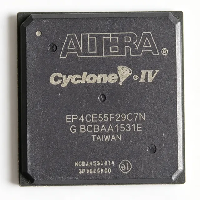
EP4CE55F29C7N - 55K LE Cyclone IV E FPGA, 780-FBGA | Intel
MPN: EP4CE55F29C7N ✓ Active| Qty | Unit Price | Extended |
|---|---|---|
| 1 | $215 | $215.00 |
| 10 | $195 | $1,950.00 |
| 100 | $175 | $17,500.00 |
| 500 | $155 | $77,500.00 |
| 1,000 | $138 | $138,000.00 |
EP4CE55F29C7N Overview
An FPGA (Field-Programmable Gate Array) is a programmable logic device composed of an array of configurable logic blocks (CLBs), programmable interconnect, and I/O cells, all of which the designer configures after manufacture using an HDL (Hardware Description Language) such as Verilog or VHDL. FPGAs sit at the same level of the programmable-logic hierarchy as CPLDs (Complex Programmable Logic Devices) but offer vastly greater logic capacity and embedded memory, and they belong to the broader semiconductor family of programmable logic ICs. The Cyclone IV E sub-family is Intel's low-power, low-cost line of SRAM-based FPGAs optimized for volume production in industrial, consumer, and automotive markets.
Key features include 2,396,160 bits of embedded SRAM organized as M9K blocks, up to 374 user I/O pins supporting multiple I/O standards (LVDS, LVTTL, LVCMOS, SSTL, HSTL), and up to 4 PLLs (Phase-Locked Loops) for clock management. The device supports Nios II embedded processor soft cores, allowing designers to integrate a 32-bit RISC microcontroller directly into the FPGA fabric. Configuration is via JTAG, Active Serial, or Passive Parallel modes, with built-in decompression and encryption engines protecting design IP.
Typical applications include industrial motor control and robotics, video processing and image pipelines, automotive driver-assistance subsystems, communications infrastructure, and consumer electronics that require custom logic, DSP, or high-speed parallel interfaces. The -7 speed grade (C7) places it in the mid-performance tier of the Cyclone IV E family, balancing timing margin against cost for mainstream designs.
When designing with this device, ensure PCB layout accommodates the 1.0 mm-pitch FBGA with appropriate microvia stack-up and decoupling strategy. Power estimation with the Intel Quartus Prime Early Power Estimator is strongly recommended before final pin assignment, since core and I/O supply currents vary significantly with logic utilization and toggle rates.
Drop-in alternatives for EP4CE55F29C7N — same package, pin-to-pin compatible. Different-package parts requiring PCB rework are excluded.
Variants in this series
Same-series models that are drop-in compatible with EP4CE55F29C7N (same form factor and footprint) — differing in Package, Speed Grade, Process Technology, Configuration Modes, Embedded 18x18 Multipliers.
Quick Comparison Tool — Select alternative parts for side-by-side comparison:
EP4CE55F29C8N
✓ In Stock
$285 / Unit
View Datasheet →EP4CE55F29C6N
✓ In Stock
$49.95 / Unit
View Datasheet →EP4CE55F29I7N
✓ In Stock
$154.8 / Unit
View Datasheet →EP4CE55F29C7
✓ In Stock
$132.4 / Unit
View Datasheet →EP4CE55F29I8LN
✓ In Stock
$165 / Unit
View Datasheet →EP4CE55F29C7N Maximum Ratings & Electrical Characteristics
| Family | Cyclone IV E |
| Logic Elements (LE) | 55,856 |
| Configurable Logic Blocks (CLBs) | 3,491 |
| Total RAM Bits | 2,396,160 |
| User I/O Count | 374 |
| Package | 780-ball FBGA (F29) |
| Package Dimensions | 29 mm x 29 mm |
| Ball Pitch | 1.0 mm |
| Operating Temperature | 0C to +85C (commercial) |
| Speed Grade | -7 (C7) |
| Core Voltage | 1.2 V nominal |
| Supply Voltage | 1.2 V |
| Mounting Type | Surface Mount |
| RoHS Status | Compliant (LEAD FREE) |
| Lead Free | Yes |
| Configuration Mode | JTAG, Active Serial, Passive Parallel |
EP4CE55F29C7N 29 mm x 29 mm Pin Configuration Guide
Pin configuration for EP4CE55F29C7N (29 mm x 29 mm package). This digital IC includes GPIO, communication interfaces (UART, SPI, I2C), and power pins. Refer to the manufacturer datasheet for alternate pin functions and configuration options. Essential for embedded system design and PCB layout.

No detailed pinout data available for EP4CE55F29C7N.
Refer to the datasheet for full pin configuration.
Typical Applications
EP4CE55F29C7N is suitable for 6 applications: Industrial Motor Control, Video and Image Processing Pipelines, Automotive Driver-Assistance Subsystems, Communications Infrastructure (Baseband / Bridging), Test and Measurement Instrumentation, Consumer Electronics and Embedded Displays.
Industrial Motor Control
The EP4CE55F29C7N's 55,856 logic elements and 374 user I/Os deliver ample capacity for multi-axis motor control designs that integrate PWM generators, encoder interfaces, and current/voltage sensing. Its 2,396,160 bits of embedded RAM (M9K blocks) support field-oriented control (FOC) lookup tables and ripple-compensation coefficients without external memory. Industrial motor drives also benefit from the LVDS and HSTL I/O support for high-speed resolver feedback. Placed as the central control FPGA, this Cyclone IV E device can drive six independent three-phase inverters while leaving headroom for safety logic and CAN / RS-485 communication. Designers can implement soft Nios II cores for housekeeping tasks alongside the deterministic hardware accelerator blocks.
Recommended
Video and Image Processing Pipelines
The EP4CE55F29C7N is widely deployed in mid-range video processing pipelines, including HD video scaling, de-interlacing, and color-space conversion. Its 18x18 hardware multipliers and dedicated memory blocks implement real-time 2D filters (FIR, sharpening) at pixel rates up to 1080p60. The 374 user I/Os accept multiple parallel RGB/YCbCr buses plus BT.656 / BT.1120 serial streams and drive HDMI, LVDS, or MIPI bridges. The 1.2 V core plus selectable I/O voltages simplify interfacing with both 1.8 V image sensors and 3.3 V display drivers. Quartus Prime DSP Builder can compile the video chain into optimized hardware with timing closure at the -7 speed grade.
Recommended
Automotive Driver-Assistance Subsystems
In ADAS (Advanced Driver-Assistance Systems) applications such as rear-view cameras, surround-view pre-processing, and ultrasonic fusion, the EP4CE55F29C7N provides parallel sensor aggregation and pre-DSP filtering. Its 2.4 Mbit embedded RAM buffers raw sensor frames before handoff to an external SoC, offloading the application processor. Multi-protocol I/O (CAN, LIN, FlexRay emulation via LVDS) supports gateway functions. For harsh-temperature under-hood installations, designers should select the -I industrial variant (EP4CE55F29I7N) which drops into the same F29 package but extends the operating range to -40C to +100C per Intel's Cyclone IV ordering guide.
Recommended
Communications Infrastructure (Baseband / Bridging)
The EP4CE55F29C7N is well-suited for protocol bridging between legacy telecom buses and modern Ethernet-based backhaul. Its high user-I/O count supports parallel TDM (Time-Division Multiplexing) interfaces, while embedded multipliers handle encryption and forward-error-correction (FEC) algorithms at line rate. The device's four PLLs (per Cyclone IV E family data) generate independent clocks for fabric, transceivers, and external PHY devices, simplifying multi-rate designs. Designers building custom CPRI or JESD207 front-ends leverage the FPGA's deterministic latency and hardware accelerators alongside Nios II soft processors for housekeeping, creating a flexible SDR (Software-Defined Radio) front-end.
Recommended
Test and Measurement Instrumentation
The EP4CE55F29C7N is a strong fit for digital test equipment where deterministic timing, parallel I/O, and on-chip DSP matter more than transceiver count. Logic-analyzer probe heads, protocol exercisers, and arbitrary waveform generators benefit from the 374 user I/Os and embedded RAM, while 18x18 multipliers accelerate FFT-based spectrum analysis. The -7 speed grade provides reliable timing closure at 200+ MHz internal fabric clocks, and Quartus Prime's TimeQuest timing analyzer ensures repeatable measurement timing across production units. JTAG-based configuration also supports in-system reprogramming during factory calibration.
Recommended
Consumer Electronics and Embedded Displays
The EP4CE55F29C7N powers consumer products such as interactive kiosks, gaming peripherals, and digital signage controllers that require custom logic, multi-touch processing, and parallel display interfaces. Its 2.4 Mbit of embedded RAM supports frame buffers and gesture-recognition lookup tables, while 374 user I/Os interface with capacitive touch controllers, RGB/LVDS panels, and audio COUs. The Cyclone IV E family is preferred over newer families for cost-sensitive consumer SKUs where the unit price of a mature silicon node outweighs the latest feature set. Designers can integrate Nios II embedded processors for application-layer logic alongside the hardware accelerator fabric.
Recommended
Recommended Products Summary
Engineering reference data for EP4CE55F29C7N — comparison, design guidance, and compliance information.
Selection Guide
Comparison with Alternatives
| Parameter | This Product | EP4CE55F29C8N | EP4CE55F29C6N | EP4CE55F29I7N | EP4CE55F29C7 | EP4CE55F29I8LN |
|---|---|---|---|---|---|---|
| Brand | Intel | Intel | Intel | Intel | Intel | Intel |
| Package | 780-FBGA (F29) | 780-FBGA (F29) - same | 780-FBGA (F29) - same | 780-FBGA (F29) - same | 780-FBGA (F29) - same | 780-FBGA (F29) - same |
| Logic Elements | 55,856 | 55,856 | 55,856 | 55,856 | 55,856 | 55,856 |
| User I/O Count | 374 | 374 | 374 | 374 | 374 | 374 |
| Embedded RAM Bits | 2,396,160 | 2,396,160 | 2,396,160 | 2,396,160 | 2,396,160 | 2,396,160 |
| Speed Grade | -7 (C7) | -8 (C8) - faster | -6 (C6) - slower | -7 (I7) | -7 (C7) | -8 (I8L) |
| Operating Temperature | 0C to +85C (commercial) | 0C to +85C (commercial) | 0C to +85C (commercial) | -40C to +100C (industrial) | 0C to +85C (commercial) | -40C to +100C (industrial) |
| RoHS / Lead-Free | Yes | Yes | Yes | Yes | Yes | Yes |
Key Differentiators
- Mid-tier density sweet spot in Cyclone IV E family (vs EP4CE40F29C7N)
- Lower unit cost than EP4CE75 / EP4CE115 in the same package (vs EP4CE75F29C7N)
- Commercial temperature grade for indoor / controlled environments (vs EP4CE55F29I7N)
Design Notes
The 780-FBGA F29 package has 1.0 mm ball pitch, which demands microvia (laser-drilled) PCB technology and a high-layer-count stack-up. Designers should use Intel's symbol and footprint libraries from the Quartus Prime installation rather than third-party footprints, since escape routing from the inner balls is non-trivial and a single mismatch can break board-to-package compatibility. Decoupling requires 0.1 uF and 0.01 uF ceramics under each power pin pair, with bulk 100 uF tantalum or polymer caps near the supply pins. A 4-6 layer PCB with continuous GND and P1V2 planes immediately below the BGA is recommended to control PDN (Power-Distribution Network) impedance.
Estimated: At typical Cyclone IV E utilization (~70% LEs, 50% RAM, 100 MHz fabric clock), the EP4CE55F29C7N draws roughly 0.8-1.2 A from the 1.2 V core supply per the Intel Early Power Estimator (EPE) tool. The 29x29 mm FBGA exposes the die through the center balls; designers should connect the central GND balls to a continuous copper pour on top and inner layers to spread heat. Forced-air cooling or a thermal pad is recommended only if utilization exceeds 80% with high toggle rates; otherwise natural convection in a well-ventilated enclosure is sufficient. Junction-to-ambient thermal resistance (theta_JA) for this package is approximately 15 C/W with a 4-layer JEDEC test board, per Intel Cyclone IV E thermal characterization data.
Three pitfalls are most common with Cyclone IV E designs. First, do NOT confuse the F29 (780-FBGA) and F23 (484-FBGA) packages - they share the same silicon die but have different pin maps and are NOT PCB-compatible. Second, ensure the configuration mode pins (MSEL[3:0]) are tied to the correct values for JTAG / Active Serial / Passive Parallel mode per the datasheet - mis-wired MSEL pins are a top cause of first-power-on failure. Third, do not neglect the CRC error checking bit in the configuration bitstream for safety-critical designs; Cyclone IV E supports 16-bit and 32-bit CRC modes that catch bitstream corruption from flash memory wear.
Estimated: Use the Quartus Prime Early Power Estimator (EPE) spreadsheet before final pin assignment to model core and I/O currents, since toggle-rate assumptions can swing power budget by 2x. For a typical 70% utilization design running 100 MHz fabric with 60% toggle rate, plan for 1.0-1.5 A on VCCINT (1.2 V core) and another 200-400 mA across VCCIO banks depending on I/O switching activity. VCCPD (1.2 V) and VCCA (2.5 V) are much lower current and can be sourced from local LDO regulators. Designers must separate VCCIO bank supplies for noise-sensitive interfaces (e.g., LVDS receivers) from high-noise outputs (e.g., LVCMOS LEDs) to minimize crosstalk.
Compliance Information
RoHS compliant and lead-free per Intel Cyclone IV ordering information and FindIC datasheet summary (LEAD FREE, PBGA780, 1 mm pitch). Industrial-temp variants (-I suffix) are not AEC-Q100 qualified; for AEC-Q100 automotive programs choose the appropriate -A grade part.
