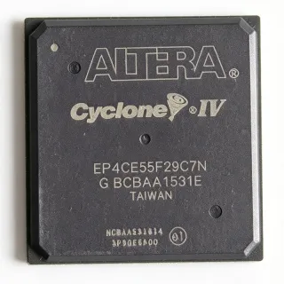
EP4CE40F29C7 - Cyclone IV E FPGA, 39.6K LE, 780-FBGA | Intel
MPN: EP4CE40F29C7 ✓ Active| Qty | Unit Price | Extended |
|---|---|---|
| 1 | $122.54 | $122.54 |
| 10 | $110.29 | $1,102.90 |
| 100 | $98.03 | $9,803.00 |
| 500 | $85.78 | $42,890.00 |
| 1,000 | $73.52 | $73,520.00 |
EP4CE40F29C7 Overview
A Field-Programmable Gate Array (FPGA) is a semiconductor integrated circuit that can be reconfigured by the customer after manufacture to implement arbitrary digital logic, DSP blocks, and memory functions. FPGAs sit hierarchically between fixed-function ASICs and software-programmable processors, combining hardware-level parallelism with software-like design iteration. The Cyclone IV E family specifically targets cost-sensitive, high-volume applications where low static power (sub-1.5 W typical) and high I/O density matter more than the highest possible logic throughput.
Key differentiating specifications include 4 embedded PLLs for clock synthesis, up to 113 embedded 18x18 multipliers for DSP, dedicated hardware for DDR/DDR2/QDR II memory interfaces, and support for LVDS, LVPECL, SSTL, and HSTL I/O standards. The device supports both asynchronous and synchronous external memory and includes configuration support via passive serial, active serial, and JTAG modes.
Architecturally, the EP4CE40F29C7 uses look-up-table (LUT) based logic blocks grouped into Logic Array Blocks (LABs), each containing 16 logic elements. Embedded memory is implemented as true dual-port M9K blocks, while DSP operations are accelerated by dedicated multiplier blocks, freeing fabric logic for control and routing. Hard PCIe, PLL, and memory controller silicon blocks reduce soft logic overhead and improve timing closure.
Typical applications include industrial motor control, video processing bridges, low-cost software-defined radio front-ends, telecom line cards, and embedded vision prototypes. The wide I/O count and DSP density also suit automotive infotainment pre-production boards and aerospace test instrumentation.
When designing with this FPGA, plan power sequencing for 1.2 V core before 2.5/3.3 V I/O, allocate sufficient decoupling (100 nF + 10 µF per supply rail), and verify JTAG chain integrity before attempting configuration. Quartus II design software (Cyclone IV device support) is required for synthesis, place-and-route, and bitstream generation.
This page synthesizes distributor pricing from DigiKey, Mouser, and Heisener, alongside drop-in same-family alternatives and engineering design notes not aggregated in any single manufacturer datasheet, providing a unique cross-reference for engineers evaluating this Cyclone IV E variant.
Drop-in alternatives for EP4CE40F29C7 — same package, pin-to-pin compatible. Different-package parts requiring PCB rework are excluded.
Variants in this series
Same-series models that are drop-in compatible with EP4CE40F29C7 (same form factor and footprint) — differing in Operating Temperature, Package, Speed Grade, Process Technology, Configuration Modes.
Quick Comparison Tool — Select alternative parts for side-by-side comparison:
EP4CE40F29C8N
✅ Drop-In✓ In Stock
$104.6 / Unit
View Datasheet →EP4CE40F29C6
✅ Drop-In✓ In Stock
$84.1 / Unit
View Datasheet →EP4CE40F29C6N
✅ Drop-In✓ In Stock
$77.51 / Unit
View Datasheet →EP4CE40F29I7N
✅ Drop-In ⚠️ 参数待验证✓ In Stock
$124 / Unit
View Datasheet →EP4CE55F29C7
✅ Drop-In✓ In Stock
$132.4 / Unit
View Datasheet →EP4CE30F29C7
✅ Drop-In📋 Reference alternative (not in catalog)
EP4CE40F29C7 Maximum Ratings & Electrical Characteristics
| Family | Cyclone IV E |
| Logic Elements (LE) | 39,600 |
| Embedded Memory Bits | 1,161,216 bits |
| Embedded 18x18 Multipliers | 113 |
| User I/O Count | 532 |
| PLLs | 4 |
| Process Technology | 60 nm (TSMC low-power) |
| Core Voltage | 1.2 V |
| I/O Voltage Support | 1.2 V / 1.5 V / 1.8 V / 2.5 V / 3.3 V |
| Package | 780-ball FBGA (F29) |
| Mounting Type | Surface Mount |
| Operating Temperature | 0C to +85C (Commercial, C7 speed grade) |
| Configuration Modes | Passive Serial, Active Serial, JTAG |
| Memory Interface Support | DDR, DDR2, QDR II, SDR |
| I/O Standards | LVDS, LVPECL, SSTL, HSTL, LVTTL, LVCMOS |
| RoHS Status | Compliant |
| Lead-Free | Yes |
EP4CE40F29C7 780-ball fbga (f29) Pin Configuration Guide
Pin configuration for EP4CE40F29C7 (780-ball fbga (f29) package). This digital IC includes GPIO, communication interfaces (UART, SPI, I2C), and power pins. Refer to the manufacturer datasheet for alternate pin functions and configuration options. Essential for embedded system design and PCB layout.

No detailed pinout data available for EP4CE40F29C7.
Refer to the datasheet for full pin configuration.
Typical Applications
EP4CE40F29C7 is suitable for 6 applications: Industrial Motor Control, Video Processing Bridge, Software-Defined Radio Front-End, Telecom Line Card Interface, Embedded Vision Prototype, Test & Measurement Instrumentation.
Industrial Motor Control
The EP4CE40F29C7 fits industrial motor control because its 39,600 logic elements and 113 embedded 18x18 multipliers close timing on 3-axis field-oriented control loops at 32 kHz PWM without external DSP. The 4 PLLs generate the precise carrier frequencies needed for sinusoidal commutation, while 532 user I/Os accommodate parallel encoder feedback and gate-driver control. Compared with a discrete MCU+FPGA split, the integrated design reduces BOM cost and PCB area. Typical design: place QDR II memory on the dedicated DDR interface for commutation lookup tables, route incremental encoder inputs through LVDS pairs, and use the hardware multipliers for Park/Clarke transforms.
Recommended
Video Processing Bridge
Video format conversion and scaling benefit from the EP4CE40F29C7's 532 I/O count and DSP blocks, which absorb wide parallel RGB/YCbCr buses and run real-time deinterlacing or color-space conversion. The 780-ball FBGA package accommodates the dense BGA-to-board routing required for 24-bit parallel video interfaces at 150 MHz pixel clock. Embedded M9K memory blocks buffer scan-line and frame data, while the dedicated DDR2 controller interfaces to external SDRAM for full-frame storage. Compared with a dedicated ASSP, this FPGA allows late-stage resolution and frame-rate changes via Quartus II recompile.
Recommended
Software-Defined Radio Front-End
Low-cost software-defined radio front-ends benefit from the EP4CE40F29C7's 113 hardware 18x18 multipliers and 1.16 Mbit of embedded memory, which together implement digital down-conversion, FIR filtering, and FFT processing at sample rates up to 80 MSPS. The 4 PLLs generate the ADC sample clock and IF LO independently, while LVDS I/O banks handle high-speed ADC/DAC data capture. The commercial C7 speed grade is sufficient for most narrowband protocols (FM, DAB, basic LTE). Power consumption stays below 1.5 W typical, making passive cooling feasible in portable SDR enclosures.
Recommended
Telecom Line Card Interface
Telecom line cards benefit from the EP4CE40F29C7's multi-standard I/O support (LVDS, LVPECL, SSTL, HSTL), which lets one device bridge legacy TDM buses, modern SERDES lanes, and backplane fabrics on a single silicon platform. The 4 PLLs derive independent clocks for each interface domain, while the dedicated DDR2 controller handles packet buffering in conjunction with external SDRAM. Compared with a bank of ASSPs, this FPGA consolidates glue logic, protocol bridges, and packet classifiers into one device, reducing board area and BOM count on dense line cards.
Recommended
Embedded Vision Prototype
Embedded vision prototypes benefit from the EP4CE40F29C7's parallel MIPI-CSI-2/LVDS sensor inputs and hardware DSP pipeline, which perform real-time edge detection, histogram equalization, or simple object detection at 30-60 fps. The 1.16 Mbit of embedded RAM buffers line-scan data without spilling to external memory, while 532 I/Os allow direct connection to image sensors without a bridge ASIC. Compared with running vision algorithms on a CPU, this FPGA delivers 10-50x speedup at the same BOM cost, making it ideal for early-stage prototype evaluation before ASIC conversion.
Recommended
Test & Measurement Instrumentation
Test and measurement instruments benefit from the EP4CE40F29C7's combination of 532 user I/Os, 4 PLLs, and 113 hardware multipliers, which together implement arbitrary waveform generation, pattern generation, and protocol-aware triggering. The LVDS I/O banks connect directly to high-speed DACs and ADCs, while the dedicated DDR2 controller streams captured waveforms to host memory via PCIe soft cores. Commercial C7 speed grade is adequate for instruments up to 200 MHz bandwidth, and the same F29 footprint is shared across the EP4CE30/40/55 family for design migration.
Recommended
Recommended Products Summary
Engineering reference data for EP4CE40F29C7 — comparison, design guidance, and compliance information.
Selection Guide
Comparison with Alternatives
| Parameter | This Product | EP4CE40F29C8N | EP4CE40F29C6 | EP4CE40F29C6N | EP4CE40F29I7N | EP4CE55F29C7 | EP4CE30F29C7 |
|---|---|---|---|---|---|---|---|
| Package | 780-ball FBGA (F29) | 780-ball FBGA (F29) - same | 780-ball FBGA (F29) - same | 780-ball FBGA (F29) - same | 780-ball FBGA (F29) - same | 780-ball FBGA (F29) - same | 780-ball FBGA (F29) - same |
| Brand | Intel | Intel | Intel | Intel | Intel | Intel | Intel |
| Logic Elements | 39,600 | 39,600 | 39,600 | 39,600 | 39,600 | 55,440 | 29,440 |
| Embedded Memory (bits) | 1,161,216 | 1,161,216 | 1,161,216 | 1,161,216 | 1,161,216 | 2,340,000 | 608,256 |
| 18x18 Multipliers | 113 | 113 | 113 | 113 | 113 | 154 | 66 |
| User I/Os | 532 | 532 | 532 | 532 | 532 | 532 | 532 |
| PLLs | 4 | 4 | 4 | 4 | 4 | 4 | 4 |
| Operating Temperature | 0C to +85C (Commercial) | -40C to +100C (Industrial) | 0C to +85C (Commercial) | 0C to +85C (Commercial) | -40C to +100C (Industrial) | 0C to +85C (Commercial) | 0C to +85C (Commercial) |
| Speed Grade | C7 | C8 | C6 | C6 | I7 | C7 | C7 |
Key Differentiators
- Highest user I/O count in mid-density Cyclone IV E tier (vs EP4CE30F29C7 (29,440 LEs))
- Direct upgrade path to higher-density family member (vs EP4CE55F29C7 (55,440 LEs))
- C7 speed grade balance of Fmax and cost (vs EP4CE40F29C6 (C6 speed grade))
Design Notes
The EP4CE40F29C7 requires a tightly regulated 1.2 V core supply capable of delivering up to 1.5 A peak during configuration transitions. Power-sequence the 1.2 V core before the 2.5/3.3 V I/O banks to prevent back-powering through ESD diodes, which can cause latch-up. Place 100 nF ceramic decoupling within 5 mm of every VCCINT/VCCIO pin, plus a bulk 10 µF tantalum or polymer cap per supply rail. Designers using the Cyclone IV device handbook recommendation should budget for at least 4-layer PCB with a dedicated ground plane.
Estimated: At a typical industrial workload (50% logic utilization, 100 MHz clock, DDR2 interface active), the EP4CE40F29C7 dissipates roughly 1.0 to 1.4 W. The 780-ball FBGA has a theta_JA of approximately 15 C/W on a 4-layer JEDEC test board, giving a junction-to-ambient rise of 15-21C. For enclosed designs with poor airflow, derate to C6 speed grade or attach a small copper heat spreader over the top of the BGA. Always cross-check with the official Cyclone IV thermal model for your specific board stack-up.
The 780-ball F29 FBGA has a 1.0 mm ball pitch requiring laser-drilled microvia stack-ups or 4-mil trace/space on outer layers. Route all differential pairs (LVDS, LVPECL) with 100 ohm differential impedance and length matching within 150 mils. Keep the JTAG chain (TCK/TMS/TDO/TDI) under 6 inches total to avoid signal integrity issues at 30 MHz configuration clock. Provide a clear keep-out zone beneath the BGA for escape vias; Intel provides reference PCB stack-ups in AN 542.
Three pitfalls to avoid: (1) Do not program the EPCS configuration flash with a bitstream larger than 16 Mbit without using EPCQ devices - the EPCS auto-detect logic will reject mismatched densities. (2) Do not leave unused I/O banks floating - configure as output drive low or input tri-state with weak pull-up to prevent oscillation. (3) Do not skip the CONF_DONE pull-up resistor; without it, the FPGA may fail to assert configuration done and appear non-responsive. Refer to the Cyclone IV Configuration Handbook for full checklists.
Compliance Information
RoHS and lead-free status confirmed via distributor listings. Halogen-free status not explicitly listed in available data - marked unknown. Cyclone IV E family is not AEC-Q100 qualified; for automotive applications, consider Cyclone IV GX or later families.