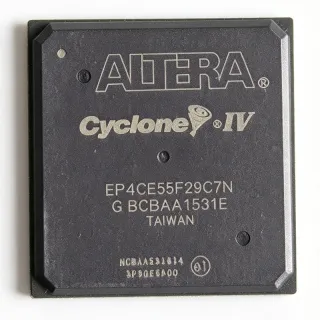
EP4CE30F29I7N - 28.8KLE Cyclone IV E FPGA 780-BGA | Intel
MPN: EP4CE30F29I7N ✓ Active| Qty | Unit Price | Extended |
|---|---|---|
| 1 | $72.06 | $72.06 |
| 10 | $65.5 | $655.00 |
| 100 | $58.2 | $5,820.00 |
| 500 | $52.1 | $26,050.00 |
| 1,000 | $47.85 | $47,850.00 |
EP4CE30F29I7N Overview
A Field-Programmable Gate Array (FPGA) is a class of programmable logic device (PLD) that allows engineers to implement arbitrary digital logic functions through configurable logic blocks (CLBs), programmable interconnects, and dedicated hardware blocks such as multipliers and memory. Within the semiconductor hierarchy, an FPGA sits below an ASIC in performance-per-watt but above discrete glue logic in integration density, making it ideal for mid-volume designs, prototyping, and applications requiring post-production firmware updates. The Cyclone IV E family specifically targets cost-sensitive, low-power, high-volume applications.
Key features include 28,848 LEs, 608 Kbits of embedded RAM (M9K blocks), 532 maximum user I/Os, 66 embedded 18x18 multipliers (approximately 132 9x9 multipliers), 4 PLLs, and 20 global clock networks. The device supports LVDS, LVCMOS, SSTL, and HSTL I/O standards with on-chip termination (OCT) for signal integrity in high-speed parallel interfaces.
Architecturally, the EP4CE30F29I7N leverages a 60 nm low-k dielectric CMOS process with a 1.0V core voltage (VCCINT) and 1.2V to 3.3V tolerant I/O banks. The 8 I/O banks operate independently, allowing mixed-voltage interfacing on the same die - a critical capability for bridging legacy 5V-tolerant peripherals with modern low-voltage processors.
Typical applications include industrial motor control and factory automation, video surveillance and image processing, telecommunications line cards and protocol bridging, automotive infotainment prototypes, and low-cost ASIC prototyping. Its balance of logic density and power efficiency positions it for portable and thermally constrained embedded systems.
When designing with this device, allocate at least 8 PCB layers for the 780-BGA breakout and follow Intel's pinout guidelines for power decoupling - 100uF bulk plus 0.1uF and 0.01uF high-frequency ceramics within 100 mils of every VCCINT/VCCIO ball. JTAG access for configuration and debug should be brought out to a standard 10-pin header.
This page synthesizes distributor pricing, configuration tool links, drop-in same-brand alternatives, and practical hardware design notes not consolidated on the manufacturer product page.
Drop-in alternatives for EP4CE30F29I7N — same package, pin-to-pin compatible. Different-package parts requiring PCB rework are excluded.
Variants in this series
Same-series models that are drop-in compatible with EP4CE30F29I7N (same form factor and footprint) — differing in Package, Configuration Modes, Operating Temperature, Process Technology, Mounting Type.
Quick Comparison Tool — Select alternative parts for side-by-side comparison:
EP4CE30F29I7
✅ Drop-In📋 Reference alternative (not in catalog)
EP4CE30F29C7N
✅ Drop-In📋 Reference alternative (not in catalog)
EP4CE30F29C8N
✅ Drop-In📋 Reference alternative (not in catalog)
EP4CE30F29I8N
✅ Drop-In📋 Reference alternative (not in catalog)
EP4CE75F29I7N
✅ Drop-In✓ In Stock
$540 / Unit
View Datasheet →EP4CE30F29I7N Maximum Ratings & Electrical Characteristics
| Series | Cyclone IV E |
| Logic Elements | 28,848 |
| Embedded Memory (M9K Blocks) | 608,256 bits (66 M9K blocks) |
| Maximum User I/Os | 532 |
| Embedded 18x18 Multipliers | 66 |
| Phase-Locked Loops (PLLs) | 4 |
| Global Clock Networks | 20 |
| Process Technology | 60 nm low-power CMOS |
| Core Voltage (VCCINT) | 1.0 V (nominal), 1.2 V (performance) |
| I/O Voltage Standards | LVDS, LVCMOS, SSTL, HSTL (1.2V to 3.3V) |
| I/O Banks | 8 |
| Package | 780-ball FBGA (F29) |
| Operating Temperature (Junction) | -40C to +100C (industrial I7) |
| Speed Grade | 7 |
| Configuration Modes | Passive Serial, Active Serial, JTAG |
| RoHS Status | Compliant |
| Mounting Type | Surface Mount |
EP4CE30F29I7N 780-ball fbga (f29) Pin Configuration Guide
Pin configuration for EP4CE30F29I7N (780-ball fbga (f29) package). This digital IC includes GPIO, communication interfaces (UART, SPI, I2C), and power pins. Refer to the manufacturer datasheet for alternate pin functions and configuration options. Essential for embedded system design and PCB layout.

No detailed pinout data available for EP4CE30F29I7N.
Refer to the datasheet for full pin configuration.
Typical Applications
EP4CE30F29I7N is suitable for 7 applications: Industrial Motor Control and Factory Automation, Video Surveillance and Image Processing Pipelines, Telecommunications Line Cards and Protocol Bridging, Low-Cost ASIC Prototyping and Emulation, Automotive Infotainment and Driver Assistance Prototypes, Portable and Power-Constrained Embedded Systems, LED Display Walls and Video Signage Controllers.
Industrial Motor Control and Factory Automation
The EP4CE30F29I7N's 28,848 logic elements and 66 embedded 18x18 multipliers are well-matched to multi-axis servo and stepper motor control loops, where each axis consumes roughly 1,500 to 2,500 LEs plus a hardware multiplier for field-oriented control (FOC) algorithms. Its 532 user I/Os provide ample headroom for incremental encoder inputs (typically 4 pins per axis), PWM outputs, and opto-isolated GPIO interfacing to 24V industrial busses. The industrial -40C to +100C junction range enables deployment in unshielded factory cabinets. Compared with a DSP-based controller, the FPGA delivers deterministic single-cycle latency on the current-loop interrupt, critical for sub-microsecond torque response in high-bandwidth servo drives.
Recommended
Video Surveillance and Image Processing Pipelines
With 532 user I/Os and 66 18x18 multipliers, the EP4CE30F29I7N can ingest parallel camera sensor data (LVDS or sub-LVDS at up to 800 Mbps per pair) and perform real-time preprocessing such as color-space conversion, gamma correction, and 5x5 convolution filters for edge detection. The 608 Kbits of embedded M9K memory serves as line buffers for 1080p video at 60 fps, where each scan line requires roughly 4 Kbits per color channel. The 780-ball FBGA package routes LVDS pairs with matched impedance, and Quartus II's ALTLVDS megafunction simplifies PHY instantiation. Designers moving from ASIC to FPGA for surveillance IP cameras often select this part for its deterministic latency and reconfigurable ISP pipeline.
Recommended
Telecommunications Line Cards and Protocol Bridging
The EP4CE30F29I7N's 8 independent I/O banks support mixed-voltage operation, allowing the FPGA to bridge between 1.8V LVDS SERDES interfaces, 2.5V SSTL memory, and 3.3V LVCMOS control logic on the same die. Its 4 PLLs can synthesize independent clock domains for TDM backplanes, SDH/SONET line cards, or Ethernet PHY interfaces. The 20 global clock networks and 66 hardware multipliers accelerate forward-error-correction (FEC) and Reed-Solomon encoding typical in telecom bridge devices. Compared with discrete glue logic, the FPGA replaces dozens of bus transceivers and CPLDs while adding on-chip flexibility for evolving protocol revisions.
Recommended
Low-Cost ASIC Prototyping and Emulation
The 28,848 LEs of the EP4CE30F29I7N provide enough capacity to prototype mid-complexity ASICs (typically up to 500K gates) in a single device, with deterministic compile times and Quartus II's incremental compile flow preserving timing closure between iterations. The 780-ball FBGA offers abundant I/O for ASIC pinout replication, and the industrial temperature range supports bring-up in thermal chambers. Compared with ASIC NRE cost ($1M+ for 65 nm masks), a Cyclone IV E prototype board is typically below $500 - making this part a standard choice for ASIC functional verification and firmware development prior to tape-out.
Recommended
Automotive Infotainment and Driver Assistance Prototypes
The EP4CE30F29I7N's -40C to +100C industrial temperature range suits automotive cabin environments, where ambient temperatures reach +85C with solar load. Its 66 hardware 18x18 multipliers enable real-time object detection preprocessing in ADAS prototypes, and the 608 Kbits of embedded RAM buffer LVDS camera frames at 30 fps. The 532 user I/Os allow direct connection to multiple MIPI-CSI2 bridges, CAN transceivers, and LVDS display panels. Compared with a microcontroller + DSP combination, the single-chip FPGA solution reduces BOM, simplifies PCB layout, and enables post-production feature additions via partial reconfiguration.
Recommended
Portable and Power-Constrained Embedded Systems
The Cyclone IV E family is fabricated on a 60 nm low-power process, allowing the EP4CE30F29I7N to operate at static currents below 100 mA in low-activity designs - making it attractive for battery-powered instruments and handheld test equipment. Its 532 user I/Os accommodate LCD interfaces, USB PHY bridges, and analog front-end ADCs without external bus switches. The 4 PLLs allow fine-grained clock gating to minimize dynamic power, and Quartus II's PowerPlay analyzer reports per-bank power estimation for thermal budgeting. Compared with a Cyclone V or Stratix device, the Cyclone IV E offers 30-40% lower static power at equivalent utilization.
Recommended
LED Display Walls and Video Signage Controllers
The EP4CE30F29I7N's 532 user I/Os and 66 hardware 18x18 multipliers are well-suited to multi-output LED display controllers driving HUB75 or HUB75E panels at high refresh rates (typically 1920 Hz or higher). Each panel output requires roughly 13 GPIO signals plus clock, so a 4K video wall with 8 panel chains consumes about 104 I/Os - well within the FPGA's budget. The 4 PLLs generate multiple pixel clock domains for heterogeneous panel resolutions, and the embedded M9K memory blocks buffer scan-line data for tear-free playback. The industrial temperature range supports outdoor LED cabinet installations where temperatures exceed +60C in direct sunlight.
Recommended
Recommended Products Summary
Engineering reference data for EP4CE30F29I7N — comparison, design guidance, and compliance information.
Selection Guide
Comparison with Alternatives
| Parameter | This Product | EP4CE30F29I7 | EP4CE30F29C7N | EP4CE30F29C8N | EP4CE30F29I8N | EP4CE75F29I7N |
|---|---|---|---|---|---|---|
| Brand | Intel | Intel | Intel | Intel | Intel | Intel |
| Package | 780-ball FBGA (F29) | 780-ball FBGA (F29) - same | 780-ball FBGA (F29) - same | 780-ball FBGA (F29) - same | 780-ball FBGA (F29) - same | 780-ball FBGA (F29) - same |
| Logic Elements | 28,848 | 28,848 | 28,848 | 28,848 | 28,848 | 75,408 |
| Embedded Memory | 608,256 bits | 608,256 bits | 608,256 bits | 608,256 bits | 608,256 bits | 4,266,624 bits |
| Maximum User I/Os | 532 | 532 | 532 | 532 | 532 | 528 |
| 18x18 Multipliers | 66 | 66 | 66 | 66 | 66 | 174 |
| PLLs | 4 | 4 | 4 | 4 | 4 | 4 |
| Temperature Grade | Industrial (-40C to +100C) | Industrial (-40C to +100C) | Commercial (0C to +85C) | Commercial (0C to +85C) | Industrial (-40C to +100C) | Industrial (-40C to +100C) |
| Speed Grade | 7 | 7 | 7 | 8 | 8 | 7 |
Key Differentiators
- Industrial temperature range with same 780-BGA pinout (vs EP4CE30F29C7N)
- Higher logic density with same footprint (vs EP4CE30F29I7 (same package, identical LE count))
- Lead-free RoHS-compliant termination (vs EP4CE30F29I7 (non-N variant))
- Higher logic density upgrade path (vs EP4CE75F29I7N)
Design Notes
The 780-ball FBGA (F29) package requires an 8-layer PCB minimum with 0.4 mm ball pitch. Use a 1-4-1 or 2-4-2 stack-up with dedicated ground planes on layers 2 and 7. Per Intel's Cyclone IV Hardware Design Guidelines, allocate at least 6 vias per power ball for VCCINT (1.0V) and VCCIO (variable) to handle the inrush current during power-up, and place 100uF bulk capacitors within 1 inch of the device.
Estimated: at 50% logic utilization toggling at 100 MHz, the EP4CE30F29I7N core current is approximately 500 mA to 800 mA from the 1.0V VCCINT rail, requiring an LDO or DC-DC converter capable of 1 A continuous. The I/O banks collectively may draw 300 mA to 1.2 A depending on switching activity and bank voltage. Use PowerPlay early in the design cycle to budget exact current and select regulators with adequate thermal headroom.
For LVDS pairs (clock and data), match trace lengths within 50 mils and maintain 100 ohm differential impedance. Keep LVDS traces on the top layer or adjacent reference plane layers to minimize skew. Configure on-chip termination (OCT) via the Quartus II Assignment Editor for each LVDS pair. JTAG signals (TCK, TMS, TDI, TDO) should be routed with 4.7k pull-ups on TMS and TDI to prevent false configuration during power-up glitches.
Do not confuse the EP4CE30F29I7N (780-BGA, 532 I/O) with the EP4CE30F23I7N (484-BGA, 328 I/O) - their land patterns are different and PCB swap will cause I/O bank pinout mismatches. Also note that the F29 'I7' suffix means industrial temperature (-40C to +100C junction) AND speed grade 7; the C7 variant is commercial (0C to +85C) at the same speed grade. Verify both the package code (F29 vs F23) and temperature code (I vs C) before ordering.
Estimated: with theta_JA around 14 C/W on a JEDEC 4-layer test board, the EP4CE30F29I7N can dissipate approximately 7W before exceeding the +100C industrial junction limit in still air. For designs exceeding 3W total power, add a 50 mm x 50 mm copper heatsink or forced-air cooling. Use the Thermal Resistance Calculator in PowerPlay to validate your specific PCB stack-up and enclosure conditions.
Compliance Information
RoHS-compliant lead-free (Pb-free) ball termination per 'N' suffix; not AEC-Q100 qualified (industrial grade only); halogen-free status not explicitly stated in provided data - confirm with manufacturer datasheet.