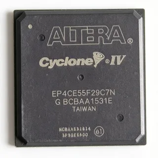
EP4CE55F29C8N - Cyclone IV E FPGA, 55K LE, 780-BGA | Intel
MPN: EP4CE55F29C8N ✗ End of Life| Qty | Unit Price | Extended |
|---|---|---|
| 1 | $385 | $385.00 |
| 10 | $360 | $3,600.00 |
| 100 | $330 | $33,000.00 |
| 500 | $305 | $152,500.00 |
| 1,000 | $285 | $285,000.00 |
EP4CE55F29C8N Overview
A Field Programmable Gate Array (FPGA) is a semiconductor integrated circuit built around a matrix of configurable logic blocks (CLBs), programmable interconnect, and dedicated hard IP such as block RAM, DSP blocks, and PLL/IO controllers. Unlike an ASIC, an FPGA's logic function and routing are defined after manufacturing by loading a user bitstream into SRAM configuration cells. FPGAs sit at the top of the programmable logic hierarchy: programmable logic device (PLD) > CPLD > FPGA > SoC FPGA, with Cyclone IV E positioned as Intel's lowest-power, lowest-cost Cyclone generation, optimized for high-volume cost-sensitive designs.
Key Cyclone IV E features include up to 15,408 Kbits of embedded memory, hardware DSP blocks for high-throughput arithmetic, eight PLLs per device for flexible clock synthesis, and support for external memory interfaces including DDR, DDR2, and QDRII SRAM. The 8 in the suffix indicates a commercial temperature grade (0 C to +85 C) and speed grade 8, while F29 denotes the FBGA-780 package code.
The Cyclone IV E architecture combines a 4-input ALM-based logic fabric with embedded M9K memory blocks and 18x18 hardware multipliers. This balance of fabric and hard IP delivers strong DSP throughput at low static and dynamic power, and allows the same silicon to serve cost-driven control planes and moderate-throughput signal-processing pipelines.
Typical applications include industrial motor control and PLCs, video surveillance and image processing front-ends, automotive infotainment and driver-assist prototypes, portable medical instrumentation, and low-cost ASIC prototyping. The wide operating temperature range and proven Quartus Prime II tool support make EP4CE55F29C8N a frequent choice for production designs migrated from larger Cyclone III devices.
Designers should be aware that Cyclone IV E is in NRND/EOL status; pin-compatible migration paths include Cyclone IV GX (with transceivers), Cyclone V E (28 nm, lower power), and MAX 10 for non-transceiver cost reduction. Always validate Quartus software support before starting a new design.
This page consolidates current distributor pricing, same-family drop-in variants, and design considerations not found in a single datasheet - including a comparison of all FBGA-780 Cyclone IV E density and speed-grade options.
Drop-in alternatives for EP4CE55F29C8N — same package, pin-to-pin compatible. Different-package parts requiring PCB rework are excluded.
Variants in this series
Same-series models that are drop-in compatible with EP4CE55F29C8N (same form factor and footprint) — differing in Package, Speed Grade, Process Technology, Embedded 18x18 Multipliers, Operating Temperature.
Quick Comparison Tool — Select alternative parts for side-by-side comparison:
EP4CE55F29C8LN
✅ Drop-In✓ In Stock
$78.9 / Unit
View Datasheet →EP4CE55F29C7N
✅ Drop-In✓ In Stock
$138 / Unit
View Datasheet →EP4CE55F29C6N
✅ Drop-In✓ In Stock
$49.95 / Unit
View Datasheet →EP4CE40F29C8N
✅ Drop-In✓ In Stock
$104.6 / Unit
View Datasheet →EP4CE115F29C8N
✅ Drop-In✓ In Stock
$38.9 / Unit
View Datasheet →EP4CE55F29C8N Maximum Ratings & Electrical Characteristics
| Family | Cyclone IV E |
| Logic Elements (LE) | 55,856 |
| Embedded Memory | 2,340 Kbits |
| Embedded Multiplier Blocks (18x18) | 154 |
| Maximum User I/O Pins | 374 |
| Logic Array Blocks (LABs) | 3,491 |
| Process Technology | 60 nm (TSMC low-power) |
| Core Voltage | 1.2 V |
| Package | 780-ball FBGA (F29) |
| Mounting Type | Surface Mount |
| Speed Grade | 8 (commercial) |
| Temperature Grade | Commercial (0 C to +85 C) |
| PLLs | 4 to 8 (per device) |
| Configuration Method | SRAM-based, volatile (requires external config device) |
| RoHS Status | Compliant |
| Lead-Free / Halogen-Free | Yes (per part marking) |
EP4CE55F29C8N 780-ball fbga (f29) Pin Configuration Guide
Pin configuration for EP4CE55F29C8N (780-ball fbga (f29) package). This digital IC includes GPIO, communication interfaces (UART, SPI, I2C), and power pins. Refer to the manufacturer datasheet for alternate pin functions and configuration options. Essential for embedded system design and PCB layout.

No detailed pinout data available for EP4CE55F29C8N.
Refer to the datasheet for full pin configuration.
Typical Applications
EP4CE55F29C8N is suitable for 6 applications: Industrial Motor Control & PLC, Video Surveillance / Image Processing Front-End, ASIC Prototyping & Emulation, Automotive Infotainment & Driver-Assist Prototypes, Portable Medical Instrumentation, LED Display & Signage Controllers.
Industrial Motor Control & PLC
EP4CE55F29C8N is well suited to multi-axis industrial motor control and PLC platforms, where its 55,856 logic elements comfortably host encoder decoding, current-loop PI controllers, and EtherCAT/EtherNet/IP MACs in soft logic. With 154 hardware 18x18 multipliers, it can also implement field-oriented control (FOC) and SVPWM for three-phase inverters without taxing fabric DSP resources. The 374 user I/O pins handle multiple encoder inputs, gate-driver PWMs, and parallel ADC/DAC buses. Designers typically pair the FPGA with external gate drivers and current-sense ADCs; Quartus II Qsys accelerates peripheral integration. Commercial temperature grade (0 to +85 C) covers most factory-floor enclosures, but for outdoor or unconditioned cabinets the industrial-speed EP4CE55F29I8N is preferred. EP4CE55F29C8N's wide NRND inventory also makes it attractive for sustaining legacy production lines without redesign.
Recommended
Video Surveillance / Image Processing Front-End
In cost-sensitive video surveillance and image-processing pipelines, EP4CE55F29C8N acts as a pre-DSP front-end that performs sensor interfacing, color-space conversion, scaling, and noise reduction before passing pixels to a host SoC or compression engine. The 55,856 LE / 2,340 Kbit embedded memory fabric is enough for two parallel 1080p60 channels with 3-tap de-noising, and the device's LVDS and DDR2 interfaces accept raw Bayer data directly from CMOS sensors. The 780-ball FBGA provides 374 user I/Os, ample for multi-sensor aggregation. Compared with a dedicated image signal processor, the FPGA gives OEMs the flexibility to differentiate via proprietary noise-reduction or analytics IP while keeping BOM cost predictable. NRND status means volume designs should migrate to Cyclone V E or MAX 10 to ensure long-term supply.
Recommended
ASIC Prototyping & Emulation
Engineers use EP4CE55F29C8N as a building block in multi-FPGA ASIC prototyping because Quartus II supports incremental compile, partition swap, and TimeQuest timing closure workflows. Each 55,856-LE device can host approximately 10-15 million gates of synthesized logic depending on clock domains and memory usage, and the FBGA-780 package exposes enough I/O to map ~370 ASIC signals per chip. DDR2 controller IP and the 154 hardware 18x18 multipliers let designers validate SoC peripherals and DSP blocks at near-real-time speeds. Compared with a single large FPGA, multiple EP4CE55 devices split the design across packages, simplifying PCB layout and reducing per-board cost. The same bitstream compatibility across speed grades 8/7/6 also helps engineers trade speed for cost on prototype versus validation builds.
Recommended
Automotive Infotainment & Driver-Assist Prototypes
Automotive Tier-1 suppliers use EP4CE55F29C8N in pre-production infotainment head units, instrument clusters, and entry-level driver-assist prototypes that need fast time-to-market with custom video and sensor pipelines. The device's LVDS, DDR2, and parallel RGB interfaces support LVDS-display aggregation, surround-view stitching, and parking-camera muxing, while 55K LE accommodate H.264 encode assist or graphics overlay logic. The commercial temperature grade (0 C to +85 C) suits cabin electronics but not under-hood or windshield-mounted modules. For series production, designers typically migrate to AEC-Q100-qualified Cyclone V or Cyclone 10 devices; the EP4CE55F29C8N is used for pre-A sample builds and DV/PV validation. Quartus II automotive IP cores ease CAN, LIN, and FlexRay bridging.
Recommended
Portable Medical Instrumentation
Portable patient monitors, ultrasound front-ends, and point-of-care diagnostics leverage EP4CE55F29C8N for its balance of DSP bandwidth, low static power, and rich IP ecosystem. With 154 hardware multipliers, the FPGA runs real-time FIR/IIR filtering, beamforming, and pulse-oximetry algorithms without offloading to a host CPU. The 2,340 Kbit embedded memory holds multiple line buffers for ultrasound beamforming or ECG sample windows, while the 374 user I/Os interface to high-speed ADCs and LCD displays. The commercial temperature range covers clinical environments (typically 0 to +50 C); medical OEMs typically add IEC 60601-1 system-level certification around the FPGA rather than relying on device qualifications alone. NRND status means new medical designs should consider MAX 10 or Cyclone V E for assured long-term supply.
Recommended
LED Display & Signage Controllers
Large-format LED video walls, stadium scoreboards, and outdoor digital-signage controllers use EP4CE55F29C8N to aggregate multiple HDMI/DisplayPort inputs, perform color calibration, and drive high-channel-count LED driver chains. The 55,856 LE comfortably host 4K-to-8K pixel remapping, gamma correction, and per-cabinet brightness compensation, while 374 user I/Os provide parallel LVDS lanes to scan-row driver boards. Hardware multipliers accelerate refresh-rate conversion and 3D LUT interpolation. The 780-ball FBGA package's PCB thermal performance is adequate for the device's static power at commercial temperatures. Compared with a microcontroller + serializer approach, an FPGA-based LED controller achieves lower latency and higher refresh rates for fine-pitch (P1.5-P2.5) installations.
Recommended
Recommended Products Summary
Engineering reference data for EP4CE55F29C8N — comparison, design guidance, and compliance information.
Selection Guide
Comparison with Alternatives
| Parameter | This Product | EP4CE55F29C8LN | EP4CE55F29C7N | EP4CE55F29C6N | EP4CE40F29C8N | EP4CE115F29C8N |
|---|---|---|---|---|---|---|
| Brand | Intel | Intel | Intel | Intel | Intel | Intel |
| Package | 780-ball FBGA (F29) | 780-ball FBGA (F29) - same | 780-ball FBGA (F29) - same | 780-ball FBGA (F29) - same | 780-ball FBGA (F29) - same | 780-ball FBGA (F29) - same |
| Logic Elements | 55,856 LE | 55,856 LE | 55,856 LE | 55,856 LE | 39,600 LE (-29%) | 114,480 LE (+105%) |
| Embedded Memory | 2,340 Kbits | 2,340 Kbits | 2,340 Kbits | 2,340 Kbits | 1,134 Kbits | 3,888 Kbits |
| Speed Grade | 8 (fastest) | 8 | 7 | 6 (slowest) | 8 | 8 |
| Maximum User I/O | 374 | 374 | 374 | 374 | 532 (higher I/O) | 528 |
| Embedded 18x18 Multipliers | 154 | 154 | 154 | 154 | 116 | 266 |
| Process / Core Voltage | 60 nm / 1.2 V | 60 nm / 1.2 V | 60 nm / 1.2 V | 60 nm / 1.2 V | 60 nm / 1.2 V | 60 nm / 1.2 V |
| Lifecycle Status | NRND | NRND | NRND | NRND | NRND | NRND |
Key Differentiators
- Mid-density sweet spot in F29 FBGA-780 footprint (vs EP4CE40F29C8N)
- Highest speed grade available in Cyclone IV E commercial temperature (vs EP4CE55F29C7N)
- Lower static power than Cyclone III predecessors at same logic density (vs EP3C55F484C8N (Cyclone III legacy))
Design Notes
Estimated: EP4CE55F29C8N core power at 100% utilization with 200 MHz logic and DDR2 traffic is approximately 1.5-2.5 W. Designers should size the 1.2 V regulator for at least 3 A continuous with 100 mV peak-to-peak ripple to meet Quartus PowerPlay margin. Decouple each VCCINT pin with a 0.1 uF X7R 0402 placed within 50 mil of the ball, and add four 4.7 uF bulk caps distributed around the FBGA perimeter. PLL analog supply (VCCA_PLL) needs a ferrite-bead-isolated 2.5 V rail with its own 10 uF + 0.1 uF decoupling pair.
The 780-ball FBGA F29 package uses 1.0 mm pitch balls, requiring 4-6 layer PCB with microvia-in-pad or HDI stack-up for reliable BGA breakout. Fan-out the top layer with short traces (under 8 mm) to the inner row escape vias to minimize stub lengths on DDR2/DQS pairs. Match all DDR2 trace lengths to within +/- 25 mil and route differential DQS pairs over a continuous ground reference plane. Leave 8-10 mm of copper pour under the BGA for thermal spreading and stitch the inner ground planes with a 200 mil via grid.
Three pitfalls recur on EP4CE55F29C8N designs. (1) Forgetting an external configuration device - Cyclone IV E SRAM is volatile and the FPGA will not boot without an EPCS or EPCQ flash plus proper MSEL[3:0] strapping. (2) Driving JTAG TCK faster than 33 MHz or sharing the JTAG chain across voltage domains without level shifters - this bricks the device. (3) Treating 'commercial' temperature grade as adequate for industrial deployments - use EP4CE55F29I8N if the enclosure can exceed 70 C ambient, and derate quiescent current accordingly. Always verify the bitstream MSEL/PO flag settings in Quartus before programming.
Compliance Information
RoHS and lead-free compliance per Intel product marking; commercial temperature grade only (0 C to +85 C). Not AEC-Q100 qualified - use automotive-grade Cyclone IV or Cyclone V parts for vehicle applications. REACH compliance status confirmed at the substance level by Intel.