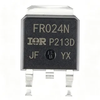
IRLR8726TRLPBF - 30V 86A N-Channel StrongIRFET™ MOSFET | Infineon
MPN: IRLR8726TRLPBF ✓ Active| Qty | Unit Price | Extended |
|---|---|---|
| 1 | $0.86 | $0.86 |
| 10 | $0.74 | $7.40 |
| 100 | $0.62 | $62.00 |
| 500 | $0.51 | $255.00 |
| 1,000 | $0.43 | $430.00 |
| 2,500 | $0.36 | $900.00 |
IRLR8726TRLPBF Overview
A power MOSFET is a voltage-controlled semiconductor switch used to efficiently route or modulate current in power conversion circuits; N-channel devices such as the IRLR8726 family conduct between drain and source when a positive gate-to-source voltage is applied. The StrongIRFET™ family is engineered for low RDS(on) per unit area and high avalanche ruggedness, optimizing the trade-off between conduction loss and switching loss that defines the figure of merit (FOM) of a power switch.
Distinguishing electrical characteristics include a logic-level VGS(th) that allows direct drive from 3.3V or 5V microcontrollers without a dedicated gate driver, 15 nC total gate charge enabling fast switching transitions, and a low 5.8 mΩ on-resistance that minimizes conduction losses even at the high currents encountered in motor drive and synchronous rectification. The DPAK package delivers these properties in a footprint familiar to industrial designers and supports wave or reflow soldering.
Architecturally, the IRLR8726 uses a stripe-cell trench gate structure with an optimized P-body region to balance RDS(on), Qg, and avalanche energy. This gives it strong performance in both hard-switched topologies (Buck, Boost) and soft-switched applications, where the low FOM reduces switching losses that dominate at high frequency.
Typical applications for the IRLR8726TRLPBF include BLDC and brushed DC motor control in cordless tools and e-bikes, low-voltage synchronous rectification in isolated DC-DC converters, high-current load switching in industrial automation, battery protection and OR-ing in 12V/24V systems, USB Power Delivery and quick-charge adapter switches, and Class-D audio amplifier output stages. The DPAK footprint makes it ideal where IPD-style integration is not desired and a discrete, thermally efficient part is preferred.
When designing with this MOSFET, place the gate drive return (source Kelvin connection where possible) as close as possible to the source pad to minimize parasitic inductance, and verify that the SOA at the application's actual VDS and pulse duration stays within the datasheet envelope; at full rated current in DPAK, a copper area of at least 1 square inch is recommended for thermal relief. According to the Infineon datasheet, the part is RoHS compliant and rated for an operating junction temperature up to 175°C.
This page combines manufacturer datasheet data, distributor pricing as of 2026-09-10, drop-in alternatives, and practical design notes that are not aggregated on a single distributor product page.
Drop-in alternatives for IRLR8726TRLPBF — same package, pin-to-pin compatible. Different-package parts requiring PCB rework are excluded.
Variants in this series
Same-series models that are drop-in compatible with IRLR8726TRLPBF (same form factor and footprint) — differing in MSL Level, Package, Operating Junction Temperature, Drain-to-Source Voltage (VDS), Technology.
Quick Comparison Tool — Select alternative parts for side-by-side comparison:
IRLR8726TRPBF
✅ Drop-In✓ In Stock
$0.32 / Unit
View Datasheet →IRFR8726TRPBF
✅ Drop-In📋 Reference alternative (not in catalog)
IRLR7833PBF
✅ Drop-In📋 Reference alternative (not in catalog)
IRFR4104PBF
✅ Drop-In📋 Reference alternative (not in catalog)
IPD031N06L3GATMA1
✅ Drop-In✓ In Stock
$0.48 / Unit
View Datasheet →BSC011N03LSIATMA1
✅ Drop-In✓ In Stock
$1.32 / Unit
View Datasheet →IRLR8726TRLPBF Maximum Ratings & Electrical Characteristics
| Polarity / Channel Type | N-Channel |
| Drain-Source Voltage (VDS) Max | 30 V |
| Continuous Drain Current (ID) at TC=25C | 86 A |
| On-Resistance RDS(on) Max at VGS=10V | 5.8 mOhm |
| Total Gate Charge (Qg) | 15 nC |
| Maximum Power Dissipation (PD) at TC=25C | 75 W |
| Operating Junction Temperature | -55C to +175C |
| Package | TO-252AA (DPAK) |
| Mounting Type | Surface Mount |
| Technology Family | StrongIRFET |
| RoHS Compliance | ROHS3 Compliant |
| Lead-Free | Yes (PBF suffix) |
| MSL Level | 1 (per JEDEC J-STD-020, inferred from PBF suffix and DPAK packaging) |
IRLR8726TRLPBF Pin Configuration
| Pin 1 | Gate — Gate control input (logic-level) |
| Pin 2 | Drain — Drain terminal, internally connected to the tab/back metal |
| Pin 3 | Source — Source terminal, internally connected to the tab/back metal |
Typical Applications
IRLR8726TRLPBF is suitable for 6 applications: Brushless DC (BLDC) Motor Drive, Low-Voltage Synchronous Rectification, High-Current Load Switching, Battery Protection and OR-ing, USB-PD and Quick-Charge Adapter Switch, Class-D Audio Amplifier Output Stage.
Brushless DC (BLDC) Motor Drive
The IRLR8726TRLPBF's 86A continuous drain current and 5.8 mOhm RDS(on) make it well suited for the low-side switch position in 12V/24V BLDC motor drive stages used in cordless tools, e-bikes, and small drones. In a typical three-phase inverter, three half-bridges carry the phase currents, and the IRLR8726's low Qg of 15 nC keeps switching losses modest at 20-50 kHz PWM frequencies, which directly impacts inverter efficiency and thermal budget. The DPAK package is well-proven in motor-drive layouts and gives strong second-source flexibility. The part's logic-level gate drive allows direct connection to MCU timer peripherals (or to gate-driver ICs) without bootstrap complexity, simplifying the BOM. For higher current systems, designers parallel two IRLR8726 devices per switch position.
Recommended
Low-Voltage Synchronous Rectification
In 12V-input isolated DC-DC converters (e.g., quarter-brick or sixteenth-brick point-of-load), the IRLR8726TRLPBF serves as a synchronous rectifier on the secondary side, replacing a Schottky diode to recover conduction loss. The 5.8 mOhm RDS(on) at 30A dissipates approximately 5.2W, compared to roughly 9W for a comparable Schottky diode, increasing overall converter efficiency by 1-2% at full load. The 30V VDS rating provides adequate margin above 12V rails, and the 15 nC Qg supports fast switching transitions at 100-300 kHz typical of these topologies. Designers should pair the part with a synchronous-rectifier controller IC that drives the gate with proper dead-time to prevent shoot-through.
Recommended
High-Current Load Switching
The IRLR8726TRLPBF is widely used as a low-side load switch in industrial automation, robotics, and 12V/24V automotive subsystems where currents up to 30-50A must be switched under microcontroller or CAN-FET driver control. Its 5.8 mOhm RDS(on) keeps voltage drop below 0.3V at full rated switch current, preserving headroom for downstream regulators. The 75W power dissipation rating at TC=25C, combined with DPAK's exposed tab for PCB copper heatsinking, supports sustained high-current operation without active cooling. Logic-level drive eliminates the need for a charge pump or gate-drive IC, reducing BOM cost by $0.10-$0.30 per channel in multi-channel load-switching cards.
Recommended
Battery Protection and OR-ing
The IRLR8726TRLPBF can be deployed as the active MOSFET in 12V/24V battery protection circuits, low-side disconnect switches, and OR-ing FETs for redundant power architectures. Its 30V VDS rating safely covers the 12V automotive transient envelope including load-dump events (with appropriate TVS clamping). The 5.8 mOhm RDS(on) at full battery current keeps dissipation manageable, while the logic-level gate allows direct interface to battery-management ICs. For e-bike and cordless-tool battery packs, the IRLR8726's DPAK footprint supports a compact 2-FET (high-side + low-side) protection circuit per cell string.
Recommended
USB-PD and Quick-Charge Adapter Switch
In USB Power Delivery (PD) and Qualcomm Quick-Charge adapters, the IRLR8726TRLPBF acts as the high-current VBUS switch that disconnects the load during fault conditions (OCP, OVP, OTP). Its 30V VDS handles 20V PD outputs plus transient margin, and the 5.8 mOhm RDS(on) keeps voltage drop below 0.1V at 5A, preserving tight PD voltage regulation. The 86A continuous rating comfortably supports 100W+ PD3.1 EPR power levels. Logic-level gate drive is compatible with the GPIO of mainstream PD controller ICs (e.g., FUSB302, CYPD317x). Designers should add a TVS diode for ESD and use the IRLR8726's avalanche rating to absorb switching transients.
Recommended
Class-D Audio Amplifier Output Stage
The IRLR8726TRLPBF is a popular choice for the half-bridge output stage of mid-power Class-D audio amplifiers, where its low RDS(on) minimizes conduction loss and its 15 nC Qg supports 250-500 kHz PWM switching typical of audio amplifiers. At a 4-ohm speaker load, the IRLR8726's 5.8 mOhm contributes <0.15 dB of damping-factor loss compared to an ideal switch. The DPAK package allows direct PCB heatsinking of the half-bridge without elaborate cooling. Logic-level gate drive is compatible with most Class-D modulator ICs (e.g., TPA32xx, IRS2092). For higher-power subwoofer amplifiers, two IRLR8726s can be paralleled per half-bridge position.
Recommended
Recommended Products Summary
Engineering reference data for IRLR8726TRLPBF — comparison, design guidance, and compliance information.
Selection Guide
Comparison with Alternatives
| Parameter | This Product | IRLR8726TRPBF | IRFR8726TRPBF | IRLR7833PBF | IRFR4104PBF | IPD031N06L3GATMA1 | BSC011N03LSIATMA1 |
|---|---|---|---|---|---|---|---|
| Package | TO-252AA (DPAK) | TO-252AA (DPAK) | TO-252AA (DPAK) | TO-252AA (DPAK) | TO-252AA (DPAK) | TO-252AA (DPAK) | TO-252AA (DPAK) |
| Brand | Infineon Technologies | Infineon Technologies | Infineon Technologies | Infineon Technologies | Infineon Technologies | Infineon Technologies | Infineon Technologies |
| Technology Family | StrongIRFET | StrongIRFET | StrongIRFET | StrongIRFET | HEXFET | OptiMOS | OptiMOS |
| RoHS / Lead-Free | ROHS3 Compliant / Pb-free | ROHS3 Compliant / Pb-free | ROHS3 Compliant / Pb-free | ROHS Compliant / Pb-free (PBF) | ROHS Compliant / Pb-free (PBF) | ROHS Compliant / Pb-free | ROHS Compliant / Pb-free |
Key Differentiators
- Lowest RDS(on) in 30V DPAK StrongIRFET family at 86A rating (vs IRLR7833PBF)
- Logic-level gate drive eliminates external gate driver IC (vs IRFR4104PBF (HEXFET family))
- 60V VDS upgrade path available in same package (vs IPD031N06L3GATMA1)
Design Notes
At 60A continuous drain current and 5.8 mOhm RDS(on), the IRLR8726TRLPBF dissipates roughly 20.9W as conduction loss alone. The TO-252AA (DPAK) package has a junction-to-ambient thermal resistance of approximately 50-60 C/W on a 1-square-inch 2-oz copper pad. Estimated: with TJ_max=175C and TA=60C, available TJ rise = 115C, allowing continuous dissipation of roughly 1.9-2.3W without a heatsink. For 60A operation, either increase the copper area to 4+ square inches, add an active heatsink, or parallel multiple devices. Verify thermal performance with a thermocouple on the drain tab during worst-case load testing.
Lay out the drain pad as a continuous copper pour that extends at least 1 square inch from the DPAK tab on the top layer, with thermal vias to inner copper layers to spread heat. Keep the gate trace short (<10 mm) and route it away from the drain switching node to minimize dv/dt coupling into the gate. Place a 10-100 kohm gate-source resistor (Rgs) directly between gate and source pins to prevent floating-gate turn-on during high-side switching transitions. For high-current (>30A) applications, use 2-oz or heavier copper on the source and drain layers.
Three pitfalls to avoid when designing with the IRLR8726TRLPBF. (1) Do not exceed VDS=30V including inductive transients; add a TVS diode or snubber if the circuit has significant parasitic inductance. (2) Do not assume logic-level drive is sufficient at very high di/dt; a dedicated gate driver may be needed for sub-10ns switching at >50A. (3) Do not parallel devices without individual gate resistors (typically 10-47 ohms) - mismatched Qg between devices causes uneven current sharing and possible thermal runaway.
In bridge topologies (half-bridge, full-bridge), minimize the high-side drain-to-low-side source switching loop area by placing the high-side and low-side MOSFETs adjacent with a short return-path through the bootstrap/bulk capacitor. This loop inductance directly determines VDS overshoot during switching and the gate-drive ringing observed on the low-side FET. The IRLR8726's 15 nC Qg is low enough that careful layout matters more than gate-drive strength; a 10mm reduction in loop area can cut VDS overshoot by 5-10V in a 30V design.
Compliance Information
ROHS3 Compliant per LCSC and ICComponents listings. Lead-free per PBF suffix. AEC-Q100 automotive qualification status not stated in available data - for automotive applications verify with Infineon product page.