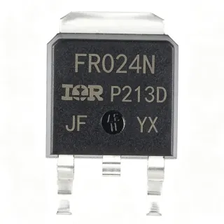
IRFR6215TRLPBF - 150V P-Ch HEXFET MOSFET, 13A, DPAK | Infineon
MPN: IRFR6215TRLPBF ✓ Active| Qty | Unit Price | Extended |
|---|---|---|
| 1 | $0.78 | $0.78 |
| 10 | $0.68 | $6.80 |
| 100 | $0.55 | $55.00 |
| 500 | $0.45 | $225.00 |
| 1,000 | $0.38 | $380.00 |
IRFR6215TRLPBF Overview
A P-channel MOSFET is a voltage-controlled device in which the source and drain terminals carry negative-polarity current relative to the source (the channel conducts when the gate is pulled below the source). MOSFETs sit one level above BJTs in the power-switching taxonomy (MOSFET -> power transistor -> discrete semiconductor) and are favored over BJTs for high-frequency switching because they are voltage-driven rather than current-driven, eliminating continuous base current and dramatically shrinking driver losses.
Key features include -150V VDS breakdown that provides generous transient headroom for 48V telecom, industrial bus, and offline-aux rails; an industry-standard DPAK footprint with an exposed drain tab for direct PCB thermal spreading; -20V maximum VGS rating with internal ESD protection; and a 175 C maximum operating junction temperature for harsh-environment survivability. The 580 mOhm maximum RDS(on) at VGS = -10V minimizes conduction loss in steady-state load-switch applications, while 44 nC Qg allows modest gate drivers to switch the device at moderate PWM frequencies.
Typical applications include high-side switching in 48V telecom and industrial bus systems, DC load management in battery-powered equipment, polarity-protection and OR-ing circuits, motor brake and slow-decay dissipation, and synchronous-rectifier replacements for PNP pass transistors in linear-regulator upgrades. The Infineon IRFR6215 family uses the same DPAK land pattern as industry-standard N-channel parts, simplifying PCB reuse for designers porting from PNP pass elements to modern MOSFET switches.
When designing with this part, observe the VGS rating: the gate must never exceed +/-20V, so a gate-resistor plus optional Zener clamp is recommended when driven by a higher-voltage gate drive. Thermal management requires copper spreading under the drain tab; a minimum 1 square inch of 2 oz copper keeps the junction within safe limits at 2-3W steady dissipation. This page synthesizes distributor pricing, drop-in alternatives, and practical design notes that complement - but do not duplicate - the manufacturer datasheet.
Drop-in alternatives for IRFR6215TRLPBF — same package, pin-to-pin compatible. Different-package parts requiring PCB rework are excluded.
Variants in this series
Same-series models that are drop-in compatible with IRFR6215TRLPBF (same form factor and footprint) — differing in Technology, RoHS Status, Package, Total Gate Charge (Qg), Drain-Source Voltage (VDS).
Quick Comparison Tool — Select alternative parts for side-by-side comparison:
IRFR6215TRRPBF
✅ Drop-In📋 Reference alternative (not in catalog)
IRFR6215PBF
✅ Drop-In📋 Reference alternative (not in catalog)
IRFR6215TRPBF
✅ Drop-In✓ In Stock
$0.65 / Unit
View Datasheet →IRFR5505TRPBF
✅ Drop-In✓ In Stock
$0.48 / Unit
View Datasheet →IRFR3710ZTRPBF
✅ Drop-In✓ In Stock
$0.42 / Unit
View Datasheet →IRFR3710ZTRLPBF
✅ Drop-In✓ In Stock
$0.58 / Unit
View Datasheet →IRFR6215TRLPBF Maximum Ratings & Electrical Characteristics
| Polarity | P-Channel |
| Drain-Source Voltage (VDS) | -150 V |
| Continuous Drain Current (ID) at Tc=25C | -13 A |
| Gate-Source Voltage (VGS) max | ±20 V |
| RDS(on) max at VGS=-10V | 580 mOhm |
| Total Gate Charge (Qg) typ | 44 nC |
| Power Dissipation (PD) at Tc=25C | 110 W |
| Maximum Operating Junction Temperature | 175 C |
| Package | TO-252AA (DPAK) |
| Mounting Type | Surface Mount |
| Technology | HEXFET Power MOSFET (Fifth Generation) |
| MSL Level | 1 |
| RoHS Status | Compliant |
| Lead-Free | Yes |
IRFR6215TRLPBF Pin Configuration
| Pin 1 | Gate — MOSFET gate input (P-channel, drives negative relative to source) |
| Pin 2 | Drain — MOSFET drain (electrically connected to the metal tab) |
| Pin 3 | Source — MOSFET source (reference for gate drive) |
Safe Operating Area - DC
Typical Applications
IRFR6215TRLPBF is suitable for 6 applications: 48V Telecom High-Side Load Switch, Battery Polarity / Reverse-Protection Switch, Industrial 24V / 96V Bus Switch, DC Load Management in Battery-Powered Equipment, Synchronous-Rectifier Replacement for PNP Pass Transistors, Motor Brake and Slow-Decay Dissipation.
48V Telecom High-Side Load Switch
The IRFR6215TRLPBF suits 48V telecom high-side switching because its -150V VDS breakdown easily tolerates 48V bus rails plus inductive spikes from downstream LC filters. Driven with a -10V gate-source bias from a small negative charge pump or isolated gate driver, the P-channel MOSFET provides true load disconnect without the auxiliary boost supply required by N-channel high-side switches. The 580 mOhm RDS(on) limits conduction loss to 0.7W at -13A, and the 44 nC Qg allows switching at 50 kHz PWM without excessive driver loss.
Recommended
Battery Polarity / Reverse-Protection Switch
In battery polarity-protection circuits the IRFR6215TRLPBF sits in the high-side return path and blocks reverse-polarity connection by leaving its gate tied to GND through a resistor, so the channel conducts only when a correctly-polarized battery is applied. The P-channel topology eliminates the Schottky diode's 0.4-0.6V drop and halves conduction loss versus the diode alternative. The -150V rating also tolerates inductive kick-back from downstream motors or solenoids during disconnect events.
Recommended
Industrial 24V / 96V Bus Switch
Industrial automation buses operating at 24V DC or 96V DC benefit from the IRFR6215TRLPBF's 150V breakdown and 110W power dissipation rating. The P-channel HEXFET can be driven directly from logic-level opto-isolators or low-side gate drivers, simplifying isolation design. The DPAK package's exposed drain tab spreads heat directly into the PCB copper pour, sustaining 2-3W continuous dissipation with a 1 square-inch copper area. This makes the device suitable for solenoid drivers, valve actuators, and motor brake circuits.
Recommended
DC Load Management in Battery-Powered Equipment
Portable battery-powered equipment uses the IRFR6215TRLPBF as a low-side load-disconnect switch to extend battery life by cutting quiescent current draw during standby. The 44 nC gate charge enables microcontroller GPIO pins to drive the device directly through a 100-ohm gate resistor without needing a dedicated gate driver IC. With VGS(th) typically around -2V to -4V, the gate can be driven from 3.3V or 5V logic for low-voltage battery cutoff in Li-ion or lead-acid packs.
Recommended
Synchronous-Rectifier Replacement for PNP Pass Transistors
Linear regulators built around PNP pass transistors (e.g., classic LM7905-style designs) can be upgraded to a synchronous-rectifier topology using the IRFR6215TRLPBF as the pass element. The P-channel MOSFET drops only I x RDS(on) instead of VBE saturation, eliminating 0.7V of headroom and improving efficiency by 5-10% at heavy loads. The 580 mOhm RDS(on) translates to 1.2W loss at -2A compared with 1.4W for the PNP at the same current, with no base-current waste.
Recommended
Motor Brake and Slow-Decay Dissipation
Brushless DC motor controllers use the IRFR6215TRLPBF in slow-decay brake mode by switching the high-side P-channel FET to dump stored inductive energy back into the supply rail through a controlled loop. The 175C maximum junction temperature and 110W power rating handle the high instantaneous dissipation during braking transients. The P-channel placement eliminates the need for a bootstrap circuit that N-channel high-side FETs require, simplifying the gate-drive architecture.
Recommended
Recommended Products Summary
Engineering reference data for IRFR6215TRLPBF — comparison, design guidance, and compliance information.
Selection Guide
Comparison with Alternatives
| Parameter | This Product | IRFR6215TRRPBF | IRFR6215PBF | IRFR6215TRPBF | IRFR5505TRPBF | IRFR3710ZTRPBF |
|---|---|---|---|---|---|---|
| Brand | Infineon | Infineon | Infineon | Infineon | Infineon | Infineon |
| Package | TO-252AA (DPAK) | TO-252AA (DPAK) - same | TO-252AA (DPAK) - same | TO-252AA (DPAK) - same | TO-252AA (DPAK) - same | TO-252AA (DPAK) - same |
| Polarity | P-Channel | P-Channel | P-Channel | P-Channel | P-Channel | N-Channel (polarity differs) |
| VDS Breakdown | -150 V | -150 V | -150 V | -150 V | -55 V | -100 V (N-channel) |
| Continuous Drain Current | -13 A | -13 A | -13 A | -13 A | -18 A | -56 A (N-channel) |
| RDS(on) max at VGS=-10V | 580 mOhm | 580 mOhm | 580 mOhm | 580 mOhm | 110 mOhm | 9 mOhm (N-channel) |
| Total Gate Charge (Qg) | 44 nC | 44 nC | 44 nC | 44 nC | 66 nC | 110 nC |
| Power Dissipation at Tc=25C | 110 W | 110 W | 110 W | 110 W | 130 W | 140 W |
| Max Junction Temperature | 175 C | 175 C | 175 C | 175 C | 175 C | 175 C |
Key Differentiators
- Industry-standard DPAK with -150V VDS margin (vs IRFR5505TRPBF)
- P-channel high-side simplicity without bootstrap (vs IRFR3710ZTRPBF)
- Fifth Generation HEXFET low-loss switching (vs IRF9530N)
Design Notes
Estimated: at 2A continuous load with 580 mOhm RDS(on), conduction loss is I^2 x R = 2.3W. The DPAK package dissipates this safely with 1 sq-inch of 2 oz copper pour connected to the drain tab. Without copper spreading, the same 2.3W would push the junction temperature above 100C at 25C ambient. For continuous loads above 5A, add a forced-air cooling source or external heatsink.
Solder the DPAK drain tab directly to the PCB copper pour using sufficient solder paste to fill the thermal via array. Use thermal vias (0.3mm drill, 1mm pitch) under the tab to conduct heat to inner copper layers. Keep the source-trace short and wide to minimize parasitic source inductance, which can cause ringing and gate-oxide over-voltage during fast switching transitions.
Do not exceed the +/-20V VGS maximum; insert a 10-100 ohm gate resistor to limit peak gate current and add an optional 18V Zener clamp from gate to source to protect against transient over-voltage from inductive source-lead inductance. For P-channel high-side switching, ensure the gate pull-up voltage does not exceed VDS rating when the switch is OFF, otherwise the channel may partially turn on through capacitive coupling.
For PWM switching above 20 kHz, place a 100 ohm gate resistor close to the MOSFET gate pin to damp LC resonance between the gate capacitance and the gate-driver trace inductance. Without damping, gate ringing can overshoot the +/-20V VGS limit and damage the gate oxide. A ferrite bead in series with the gate is an alternative damping option for very-high-frequency designs.
Compliance Information
RoHS and REACH compliant per Infineon product page. Standard part is not AEC-Q100 qualified; consult Infineon automotive catalog for qualified alternatives. Lead-free and halogen-free per PBF suffix.