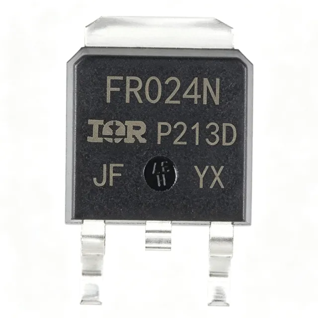
IRFR9024NTRPBF - 55V 11A P-Channel HEXFET MOSFET | Infineon
MPN: IRFR9024NTRPBF ✓ Active| Qty | Unit Price | Extended |
|---|---|---|
| 1 | $0.71 | $0.71 |
| 10 | $0.55 | $5.50 |
| 100 | $0.38 | $38.00 |
| 500 | $0.27 | $135.00 |
| 1,000 | $0.22 | $220.00 |
| 3,000 | $0.17 | $510.00 |
IRFR9024NTRPBF Overview
A P-Channel MOSFET (Metal-Oxide-Semiconductor Field-Effect Transistor) is a voltage-controlled majority-carrier device whose carrier polarity is holes (positive charge). P-Channel MOSFETs sit within the broader family of power transistors -> field-effect transistors -> MOSFETs -> discrete semiconductors. They are commonly used as high-side switches where an N-Channel driver would require a charge pump, simplifying gate-drive circuitry in load-switch and battery-protection applications.
Key features of the IRFR9024NTRPBF include advanced process technology for low RDS(on) per silicon area, a maximum continuous drain current of -11A at 25C case temperature, 38W maximum power dissipation (Tc), and an avalanche-rated body diode for inductive switching. The device is rated for operating junction temperatures from -55C to +175C, making it suitable for harsh thermal environments. The TO-252AA (DPAK) surface-mount package provides a low thermal resistance path to the PCB copper pad.
Architecturally, the IRFR9024NTRPBF uses Infineon's proprietary HEXFET fifth-generation cell structure, which optimizes the trade-off between specific on-resistance and gate charge. The P-Channel die is housed in a standard DPAK outline with the industry-standard pinout of Gate (pin 1), Drain (pin 2, tab), and Source (pin 3), allowing drop-in compatibility with numerous cross-brand equivalents.
Typical applications include high-side load switches in industrial control, battery protection and OR-ing in portable equipment, DC fan and motor speed control, power-rail inverters, and general-purpose power management in consumer and automotive 12V/24V subsystems. The P-Channel topology simplifies high-side switching without needing a bootstrap supply.
When designing with this part, ensure the gate-source drive provides at least -10V for full enhancement, and keep the dv/dt loop between drain and source compact to limit ringing. The TO-252AA tab must be soldered to a copper pour of at least 1 square inch for the rated 38W power dissipation.
Drop-in alternatives for IRFR9024NTRPBF — same package, pin-to-pin compatible. Different-package parts requiring PCB rework are excluded.
Variants in this series
Same-series models that are drop-in compatible with IRFR9024NTRPBF (same form factor and footprint) — differing in Technology, Package, Configuration, Lead-Free / RoHS, Operating Temperature Range.
Quick Comparison Tool — Select alternative parts for side-by-side comparison:
IRFR024NTRPBF
✓ In Stock
$0.31 / Unit
View Datasheet →IRFR5505TRPBF
✓ In Stock
$0.48 / Unit
View Datasheet →IRFR5505TRLPBF
✓ In Stock
$0.38 / Unit
View Datasheet →IRF7205TRPBF
✓ In Stock
$0.18 / Unit
View Datasheet →IRFR9024NPBF
📋 Reference alternative (not in catalog)
IRFR9024NTRPBF Maximum Ratings & Electrical Characteristics
| Polarity | P-Channel |
| VDS (Drain-Source Voltage) | -55 V |
| Continuous Drain Current (Tc=25C) | -11 A |
| VGS (Gate-Source Voltage) | ±20 V |
| RDS(on) Max at VGS=-10V | 175 mOhm |
| Total Gate Charge (Qg) | 12.7 nC |
| Maximum Power Dissipation (Tc=25C) | 38 W |
| Operating Junction Temperature | -55C to +175C |
| Package | TO-252AA (DPAK) |
| Mounting Type | Surface Mount |
| Pin Count | 3 |
| Technology | HEXFET (Gen 5) |
| RoHS Status | Compliant |
IRFR9024NTRPBF Pin Configuration
| Pin 1 | Gate — Gate control input |
| Pin 2 | Drain — Drain connection (electrically tied to the metal tab) |
| Pin 3 | Source — Source connection |
Safe Operating Area (DC)
Typical Applications
IRFR9024NTRPBF is suitable for 6 applications: High-Side Load Switch for 24V Industrial Bus, Battery Protection and OR-ing in Portable Equipment, DC Fan and Small Motor Speed Control, Power-Rail Inverter for Audio Amplifiers, Polarity-Reversal Protection for USB and Power Connectors, Automotive 12V Lighting and Accessory Loads.
High-Side Load Switch for 24V Industrial Bus
The IRFR9024NTRPBF serves as a high-side P-Channel load switch on 24V industrial control boards, where its -55V VDS comfortably exceeds the 30V worst-case bus voltage including transients. With -11A continuous drain current and 175 mOhm RDS(on), the device switches most relay, solenoid, and small-motor loads directly from a microcontroller GPIO without needing a charge-pump gate driver typical of N-Channel high-side switches. The DPAK tab dissipates heat into the PCB copper pour, keeping junction rise below 30C at 5A continuous load when properly soldered. Designers should gate the part with at least -10V of gate-source drive for full enhancement, and place a 100k pull-up resistor from gate to source to prevent accidental turn-on during power-up.
Recommended
Battery Protection and OR-ing in Portable Equipment
In battery packs and uninterruptible power systems, the IRFR9024NTRPBF acts as a reverse-polarity P-Channel protection switch or a low-loss OR-ing device between two DC sources. Its 175 mOhm RDS(on) at -11A yields conduction loss of only about 2.1W at full load, far lower than the Schottky-diode drop in conventional protection circuits. The P-Channel topology enables direct gate control from the system ground reference, eliminating the isolated gate drive required by N-Channel reverse-protection circuits. Designers should verify avalanche energy handling during hot-swap events, and add a TVS clamp on the drain if the load includes significant inductance.
Recommended
DC Fan and Small Motor Speed Control
The IRFR9024NTRPBF is well suited for PWM speed control of 12V/24V DC fans and small brushless motors used in consumer and industrial equipment. Its 12.7 nC total gate charge supports PWM switching frequencies up to 100 kHz with low gate-drive loss, and the HEXFET fifth-generation cell structure provides fast body-diode recovery for clean commutation. At a typical 5A motor current and 50% duty cycle, conduction losses around 0.4W keep the DPAK package within thermal limits on a modest copper pour. Engineers should observe the safe operating area at high dV/dt conditions and gate-drive loop inductance to avoid shoot-through.
Recommended
Power-Rail Inverter for Audio Amplifiers
In Class-D and Class-AB audio amplifiers, the IRFR9024NTRPBF can be used in the power-rail switching or supply-disconnect path where its low on-resistance minimizes voltage drop across the MOSFET. The DPAK package footprint matches dozens of amplifier reference designs, enabling drop-in substitution in legacy boards. Its 38W power rating provides ample headroom for short-duration peak currents up to several times the continuous rating. Designers should parallel two IRFR9024NTRPBF devices for higher-current rails and use Kelvin-source sensing for accurate current-limit feedback in protection circuits.
Recommended
Polarity-Reversal Protection for USB and Power Connectors
The IRFR9024NTRPBF provides low-loss reverse-polarity protection on USB and barrel-jack power inputs, replacing the conventional Schottky diode to save up to 700 mV of forward drop. Its P-Channel topology keeps the load on the high-side, allowing the source to sit at the input voltage and the drain to drive the downstream rail directly. The 175 mOhm on-resistance yields under 100 mV drop at 5A, preserving headroom for downstream regulators. The DPAK package handles the inrush current of hot-plug events when paired with a soft-start gate resistor.
Recommended
Automotive 12V Lighting and Accessory Loads
The IRFR9024NTRPBF handles 12V automotive lighting, horn, and accessory-switching applications where its -55V VDS provides ample margin above the 16V load-dump transient specified by ISO 7637-2. The -11A continuous rating drives most halogen and LED lighting loads and small solenoids without paralleling devices. P-Channel control from a low-side microcontroller output simplifies body-control module design by eliminating the high-side predriver stage. Designers should add a flyback diode across inductive loads and verify AEC-Q101 qualification for OEM automotive deployments.
Recommended
Recommended Products Summary
Engineering reference data for IRFR9024NTRPBF — comparison, design guidance, and compliance information.
Selection Guide
Comparison with Alternatives
| Parameter | This Product | IRFR9024NPBF | IRFR024NTRPBF | IRFR5505TRPBF | IRF7205TRPBF |
|---|---|---|---|---|---|
| Brand | Infineon | Infineon | Infineon | Infineon | Infineon |
| Package | TO-252AA (DPAK) | TO-252AA (DPAK) | TO-252AA (DPAK) | TO-252AA (DPAK) | TO-252AA (DPAK) |
| Polarity | P-Channel | P-Channel | N-Channel | P-Channel | P-Channel |
| VDS Max | -55 V | -55 V | 55 V | -55 V | -30 V |
| Continuous Drain Current | -11 A | -11 A | 17 A | -18 A | -55 A |
| RDS(on) Max at VGS=±10V | 175 mOhm | 175 mOhm | 100 mOhm | 110 mOhm | 70 mOhm |
| Maximum Power Dissipation | 38 W | 38 W | 45 W | 63 W | 110 W |
| Unit Price (Qty 1000) | $0.22 | $0.22 | $0.45 | $0.40 | $0.38 |
Key Differentiators
- Same Infineon HEXFET family, no redesign required (vs IRFR9024NPBF)
- Lower on-resistance for the same package and VDS class (vs IRFR024NTRPBF)
- Balanced cost-performance for low-current industrial loads (vs IRFR5505TRPBF)
Design Notes
Estimated: at -11A continuous drain current and VDS = -24V with VGS = -10V, power dissipation in the IRFR9024NTRPBF reaches roughly 21W. The TO-252AA (DPAK) package has a junction-to-case thermal resistance of about 3.1 C/W per the Infineon datasheet. To keep junction temperature below 150C at 25C ambient, the junction-to-ambient resistance (theta_JA) must remain under 6 C/W, which requires at least 1 square inch of 2-oz copper pour on the drain tab. Without adequate copper, derate the continuous current to roughly 4-5A in still air.
Solder the DPAK metal tab directly to a copper pad that extends through all PCB layers with thermal vias to the opposite-side copper pour. Use a 6-mil stencil and reflow within the JEDEC J-STD-020 profile for lead-free assembly. Place the gate resistor (typically 10-100 ohm) close to the gate pin to dampen parasitic ringing. Keep the high-dV/dt drain trace short and far from the gate trace to avoid Miller-effect coupling that can cause unwanted turn-on.
Do not exceed the VGS maximum of ±20V or the gate oxide will rupture permanently. Ensure the gate is never left floating - always include a pull-up or pull-down resistor of 10k-100k from gate to source to define the off-state. The body diode of the IRFR9024NTRPBF has limited reverse-recovery characteristics; for high-frequency bridge circuits, an external Schottky freewheeling diode may be needed to limit switching loss.
Compliance Information
RoHS compliant and lead-free per Infineon product page. Standard industrial grade - not AEC-Q100/101 qualified for automotive. For automotive deployments choose a specifically qualified P-Channel part.


