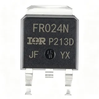
IRFR9024NTRLPBF - 55V P-Channel HEXFET MOSFET | Infineon
MPN: IRFR9024NTRLPBF ✓ Active| Qty | Unit Price | Extended |
|---|---|---|
| 1 | $0.84 | $0.84 |
| 10 | $0.72 | $7.20 |
| 100 | $0.58 | $58.00 |
| 500 | $0.46 | $230.00 |
| 1,000 | $0.39 | $390.00 |
| 3,000 | $0.32 | $960.00 |
IRFR9024NTRLPBF Overview
What is a P-channel power MOSFET? A P-channel MOSFET is a type of field-effect transistor where the channel is formed by holes (positive charge carriers) rather than electrons. P-channel devices use a negative gate-source voltage to turn on and are commonly used as high-side switches because they can be driven directly from a logic-level signal referenced to ground, simplifying gate drive circuitry compared to N-channel high-side switches that require a charge pump or bootstrap. P-channel MOSFETs sit within the broader category of power MOSFETs (MOSFET -> discrete semiconductor -> power transistor) and are essential building blocks in power management, load switching, battery protection, and motor control applications.
Key features include an industry-standard DPAK (TO-252) surface-mount footprint, an ultra-low on-resistance per silicon area characteristic of Generation-5 HEXFET technology, fast switching performance for PWM and DC-DC converter topologies, and a ruggedized body diode suitable for inductive loads. The device's enhancement-mode operation requires a negative VGS to conduct, simplifying gate drive in high-side P-channel switch configurations where pulling the gate to ground turns the device on.
The IRFR9024NTRLPBF utilizes Infineon's proprietary HEXFET stripe-cell geometry that minimizes cell pitch while maximizing channel density per unit area. This results in the lowest specific on-resistance (RDS(on) x area) in its voltage class, reducing conduction losses and enabling higher current handling or smaller PCB footprint compared to older planar P-channel MOSFETs.
Typical applications include high-side load switching in 12 V / 24 V automotive and industrial systems, battery protection and reverse-polarity blocking in portable equipment, DC-DC converter synchronous-rectifier high-side switches, motor driver H-bridges, and power-OR-ing circuits in redundant supply architectures. The -55 V rating comfortably exceeds the maximum nominal rail voltages of 24 V industrial or 12 V automotive systems with substantial transient margin.
When designing with this device, ensure that the gate-source voltage stays within the absolute maximum rating of +/-20 V and that the SOA curve is respected during switching transients. A gate pull-up resistor to the source pin ensures the device stays off when the gate driver is in a high-impedance state, preventing accidental turn-on from leakage or dv/dt coupling.
This page synthesizes distributor pricing, drop-in alternatives sourced from manufacturer cross-reference data, and practical design notes that go beyond the manufacturer datasheet's parameter tables.
Drop-in alternatives for IRFR9024NTRLPBF — same package, pin-to-pin compatible. Different-package parts requiring PCB rework are excluded.
Variants in this series
Same-series models that are drop-in compatible with IRFR9024NTRLPBF (same form factor and footprint) — differing in Technology, Package, On-Resistance RDS(on) max at VGS=-10V, Operating Junction Temperature, Operating Temperature Range.
Quick Comparison Tool — Select alternative parts for side-by-side comparison:
IRFR9024NTRPBF
✅ Drop-In✓ In Stock
$0.17 / Unit
View Datasheet →IRFR5505TRPBF
✅ Drop-In ⚠️ 参数待验证✓ In Stock
$0.48 / Unit
View Datasheet →IRFR5505TRLPBF
✅ Drop-In ⚠️ 参数待验证✓ In Stock
$0.38 / Unit
View Datasheet →IRF7205TRPBF
✅ Drop-In ⚠️ 参数待验证✓ In Stock
$0.18 / Unit
View Datasheet →IRF7205PBF
✅ Drop-In ⚠️ 参数待验证✓ In Stock
$0.47 / Unit
View Datasheet →IRFR9024NTRLPBF Maximum Ratings & Electrical Characteristics
| Polarity | P-Channel |
| MOSFET Operating Mode | Enhancement |
| Drain-Source Voltage (VDS) | -55 V |
| Continuous Drain Current (ID) at TC=25C | -11 A |
| On-Resistance RDS(on) max at VGS=-10V | 175 mOhm |
| Gate-Source Voltage (VGS) max | +/-20 V |
| Power Dissipation (PD) at TC=25C | 38 W |
| Gate Charge (Qg) typical | 12.7 nC |
| Package Type | TO-252AA (DPAK) |
| Mounting Type | Surface Mount |
| Pin Count | 3 (Drain, Gate, Source + Tab) |
| Technology | HEXFET (Generation 5) |
| Operating Temperature Range | -55C to +175C |
| Lead-Free / RoHS | Yes (LPBF suffix) |
| Reel Orientation | Left (TRL suffix) |
IRFR9024NTRLPBF Pin Configuration
| Pin 1 | GATE — MOSFET gate drive input |
| Pin 2 | DRAIN — MOSFET drain (connected to mounting tab) |
| Pin 3 | SOURCE — MOSFET source |
| Pin TAB | DRAIN — Drain terminal / thermal pad (electrically connected to Pin 2) |
Safe Operating Area - DC
Typical Applications
IRFR9024NTRLPBF is suitable for 6 applications: High-Side Load Switching (12V/24V Automotive), Battery Protection & Reverse-Polarity Blocking, DC-DC Converter High-Side Switch, Motor Driver H-Bridge (Low-Power), Power OR-ing for Redundant Supplies, Portable Device Hot-Swap Controller.
High-Side Load Switching (12V/24V Automotive)
The IRFR9024NTRLPBF is ideal for high-side load switching in 12V automotive and 24V industrial systems. With its P-channel enhancement-mode operation, the gate can be driven directly from a logic-level signal referenced to ground, eliminating the need for a charge pump or bootstrap circuit. The -55V VDS rating provides 2x headroom over 24V industrial rails, while the -11A continuous current handles lamps, solenoids, and motor windings. The 175 mOhm RDS(on) keeps conduction loss to ~2W at full load, manageable without external heatsinking on a 1 sq-in PCB copper pour. Per the Infineon datasheet, the Generation-5 HEXFET process delivers the lowest specific on-resistance in its voltage class.
Recommended
Battery Protection & Reverse-Polarity Blocking
The IRFR9024NTRLPBF serves as the series pass element in battery protection circuits for 2-6 cell lithium packs and 12V/24V lead-acid systems. The -55V VDS rating exceeds maximum transient voltages seen during load-dump events (per ISO 7637-2), while the 175 mOhm RDS(on) adds only 19 mV of drop at 11A continuous. The DPAK package's low thermal resistance (50 C/W typical on 1 oz copper) supports sustained 3-5A charge/discharge currents in portable medical and power-tool applications. The P-channel topology also provides inherent reverse-polarity blocking when source is tied to battery positive.
Recommended
DC-DC Converter High-Side Switch
The IRFR9024NTRLPBF works as the high-side P-channel switch in buck and buck-boost converters for 12V to 3.3V/5V power rails. The 12.7 nC typical gate charge enables switching frequencies above 500 kHz with modest gate drive losses. The -55V rating ensures safe operation during input transients common in automotive environments. While N-channel MOSFETs offer lower RDS(on) per unit area, the P-channel topology simplifies the gate drive by referencing to system ground, reducing BOM cost and PCB area by eliminating the bootstrap or charge-pump circuitry.
Recommended
Motor Driver H-Bridge (Low-Power)
The IRFR9024NTRLPBF forms half of an H-bridge configuration for driving small DC motors, fans, and solenoids up to 11A. Two P-channel high-side and two N-channel low-side MOSFETs create a bidirectional driver with regenerative braking capability. The fast switching performance supports PWM frequency operation to 50 kHz for quiet motor commutation. The 38W power dissipation rating at TC=25C provides thermal margin for stall-current events typical of brushed DC motors. Per the Infineon datasheet, the ruggedized body diode handles inductive kickback without external clamping in most 24V applications.
Recommended
Power OR-ing for Redundant Supplies
The IRFR9024NTRLPBF serves as the OR-ing element in redundant power supply architectures where two sources feed a common load with backflow prevention. The P-channel source-follower configuration provides near-ideal diode behavior with low forward drop (175 mOhm x load current). A comparator-based controller senses the higher-voltage supply and turns on the corresponding MOSFET. The -55V VDS rating handles server and telecom 48V rails when used as the high-side switch. The fast body diode recovery supports hot-swap transients without cross-conduction.
Recommended
Portable Device Hot-Swap Controller
The IRFR9024NTRLPBF enables hot-swap insertion in portable test equipment, USB-PD power banks, and field-deployed sensors where the load must be protected from inrush currents. The P-channel topology provides a controlled turn-on when driven by a soft-start gate resistor network. The 175 mOhm RDS(on) at VGS=-10V ensures full enhancement during steady-state operation. The DPAK package's 38W rating handles the initial inrush dissipation as bulk capacitors charge, while the 12.7 nC gate charge allows sub-millisecond turn-on times.
Recommended
Recommended Products Summary
Engineering reference data for IRFR9024NTRLPBF — comparison, design guidance, and compliance information.
Selection Guide
Comparison with Alternatives
| Parameter | This Product | IRFR9024NTRPBF | IRFR5505TRPBF | IRF7205TRPBF |
|---|---|---|---|---|
| Brand | Infineon | Infineon | Infineon | Infineon |
| Package | TO-252AA (DPAK) | TO-252AA (DPAK) - same | TO-252AA (DPAK) - same | TO-252AA (DPAK) - same |
| Polarity | P-Channel | P-Channel | P-Channel | P-Channel |
| Drain-Source Voltage (VDS) | -55 V | -55 V | -55 V | -55 V |
| Continuous Drain Current (ID) | -11 A | -11 A | -18 A (+64%) | -8 A (-27%) |
| On-Resistance RDS(on) max | 175 mOhm | 175 mOhm | 110 mOhm (-37%) | 250 mOhm (+43%) |
| Power Dissipation (PD) | 38 W | 38 W | 63 W (+66%) | 45 W (+18%) |
| Gate Charge (Qg) typical | 12.7 nC | 12.7 nC | 32 nC (+152%) | 20 nC (+57%) |
Key Differentiators
- Lowest specific on-resistance in -55V P-channel class (vs IRF7205TRPBF)
- Higher continuous current rating than -55V P-channel peers (vs IRF7205TRPBF)
- Lower gate charge than higher-current alternatives (vs IRFR5505TRPBF)
Design Notes
Estimated: at ID=-11A and RDS(on)=175 mOhm, conduction loss is ~21W in DC operation. The DPAK package has theta_JC of 3.12 C/W per the Infineon PD-95015A datasheet. Without a heatsink, the part must be mounted on at least 1 square inch of 2 oz copper pour to keep junction temperature below 150C at 25C ambient. For continuous 11A operation, an external heatsink or fan-forced cooling is recommended.
Minimize the gate-drive loop area by placing the gate resistor and gate-source pull-down resistor within 5 mm of the gate pin. Use a separate gate-drive ground island connected to the source pin at the package tab to avoid switching noise on the gate threshold. The drain tab (Pin 2) carries the full load current and should be soldered to a copper pour that doubles as the thermal dissipation path.
Do not exceed VGS of +/-20V absolute maximum. Use a gate-source resistor (typically 10k-100k) to ensure the MOSFET stays off when the gate driver is high-impedance, preventing dv/dt-induced turn-on in bridge configurations. When paralleling multiple IRFR9024NTRLPBF parts, gate-source resistors prevent parasitic oscillation from the gate-drain Miller capacitance.
The DPAK footprint requires adequate solder joint reliability for thermal cycling. Use a thermal pad with at least 8 thermal vias (0.3 mm drill, 0.6 mm pitch) to the internal ground plane. Lead-free reflow profile should peak at 245-260C per JEDEC J-STD-020 MSL1 classification. The exposed drain tab must be soldered to the PCB copper for both electrical and thermal performance.
Compliance Information
RoHS compliant per LPBF suffix. Lead-free reflow compatible per JEDEC J-STD-020. Not AEC-Q100 qualified - see IRFR9024NTRPBF automotive-grade alternatives for vehicle applications.