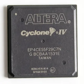
EP4CE40F29C7N - Cyclone IV E FPGA, 40K LE, 780-FBGA | Intel / Altera
MPN: EP4CE40F29C7N ✓ Active| Qty | Unit Price | Extended |
|---|---|---|
| 1 | $89.5 | $89.50 |
| 10 | $78.2 | $782.00 |
| 100 | $67.45 | $6,745.00 |
| 250 | $60.1 | $15,025.00 |
| 500 | $55.85 | $27,925.00 |
EP4CE40F29C7N Overview
What is an FPGA? An FPGA (Field Programmable Gate Array) is a semiconductor device whose digital logic function is defined after manufacturing by the user, rather than at the foundry. The device contains an array of configurable logic blocks (CLBs), programmable routing, embedded memory (BRAM), DSP blocks, and high-speed I/O and transceiver channels. FPGAs sit above microcontrollers in flexibility and below ASICs in unit cost, occupying the role of programmable hardware accelerator in the broader taxonomy: programmable logic device -> FPGA -> SRAM-based FPGA -> low-cost FPGA family.
Key features of the EP4CE40F29C7N include 4 PLLs, up to 532 user I/O pins routed through 8 I/O banks, support for external memory interfaces such as DDR/DDR2 SDRAM and QDRII SRAM, and Cyclone IV E's signature low static and dynamic power. The -7 speed grade places this device in the middle of the Cyclone IV E speed range, with internal clock frequencies reaching approximately 400-500 MHz depending on the design.
Architecturally, the Cyclone IV E family uses a 4-input LUT-based logic element, true-dual-port M9K memory blocks, and 18x18 signed multipliers that can be cascaded into larger DSP structures. The on-chip configuration controller supports both active serial (AS) and JTAG programming modes. The 780-FBGA package exposes the full I/O count of this die variant, enabling connectivity to high-bandwidth parallel buses, memory channels, and LVDS links.
Typical applications include industrial motor control and machine vision, video processing and broadcast equipment, telecommunications line cards, USB and PCIe bridging (using external PHYs), automotive infotainment prototypes, and cost-optimized ASIC prototyping. The combination of mid-range logic density, embedded multipliers, and rich memory makes the EP4CE40 well-suited for DSP-heavy designs such as software-defined radio front-ends and baseband signal processing.
When designing with this device, ensure the Quartus Prime toolchain is matched to the silicon revision, plan decoupling across all VCCINT, VCCA, and VCCIO rails, and verify pinout against the IBIS model for signal-integrity-critical I/O standards. The 780-FBGA package requires an ENIG or ENEPIG surface finish and careful via-in-pad microvia stack design.
This page synthesizes distributor pricing, drop-in same-family alternatives, and practical Quartus design notes that go beyond the Cyclone IV E Device Handbook to help engineers shorten the BOM selection and PCB bring-up cycle.
Drop-in alternatives for EP4CE40F29C7N — same package, pin-to-pin compatible. Different-package parts requiring PCB rework are excluded.
Variants in this series
Same-series models that are drop-in compatible with EP4CE40F29C7N (same form factor and footprint) — differing in Package, Operating Temperature, Speed Grade, Process Technology, Configuration Modes.
Quick Comparison Tool — Select alternative parts for side-by-side comparison:
EP4CE40F29C8N
✅ Drop-In✓ In Stock
$104.6 / Unit
View Datasheet →EP4CE40F29I7N
✅ Drop-In✓ In Stock
$124 / Unit
View Datasheet →EP4CE40F29C6N
✅ Drop-In✓ In Stock
$77.51 / Unit
View Datasheet →EP4CE40F29C7
✅ Drop-In ⚠️ 参数待验证✓ In Stock
$73.52 / Unit
View Datasheet →EP4CE40F29C7N Maximum Ratings & Electrical Characteristics
| Family | Cyclone IV E |
| Logic Elements | 39,600 |
| Embedded Memory (bits) | 1,161,216 |
| Embedded Memory Blocks (M9K) | 270 |
| DSP Blocks (18x18 Multipliers) | 116 |
| PLLs | 4 |
| Maximum User I/O | 532 |
| I/O Banks | 8 |
| Process Technology | 60 nm |
| Core Voltage (VCCINT) | 1.2 V |
| Operating Temperature | 0 C to +85 C (Commercial) |
| Speed Grade | -7 |
| Package | 780-ball FBGA (F29) |
| Mounting Type | Surface Mount (BGA) |
| MSL Level | 3 |
| RoHS Status | Compliant |
| Lead-Free | Yes |
| Configuration Mode | AS (Active Serial) / JTAG |
EP4CE40F29C7N 780-ball fbga (f29) Pin Configuration Guide
Pin configuration for EP4CE40F29C7N (780-ball fbga (f29) package). This digital IC includes GPIO, communication interfaces (UART, SPI, I2C), and power pins. Refer to the manufacturer datasheet for alternate pin functions and configuration options. Essential for embedded system design and PCB layout.

No detailed pinout data available for EP4CE40F29C7N.
Refer to the datasheet for full pin configuration.
Typical Applications
EP4CE40F29C7N is suitable for 6 applications: Industrial Motor Control and Drive, Video Processing and Image Pipeline, Telecommunications Line Card Interface, ASIC Prototyping and Emulation, USB / PCIe Bridging and Connectivity, Software-Defined Radio Baseband.
Industrial Motor Control and Drive
The EP4CE40F29C7N's combination of 116 DSP blocks, 4 PLLs, and 532 user I/O pins makes it a strong fit for multi-axis industrial motor control boards. The 18x18 hardware multipliers handle field-oriented control (FOC) loops and space-vector PWM generation in real time, while the M9K memory blocks store sine/cosine lookup tables for resolver decoding. The Cyclone IV E family is widely used in industrial servo drives, variable-frequency drives, and robotics controllers where commercial temperature grade (0C to +85C) is acceptable. Compared with a microcontroller-only solution, the FPGA off-loads deterministic control loops and leaves the MCU free for comms and housekeeping.
Recommended
Video Processing and Image Pipeline
The EP4CE40F29C7N is commonly deployed in mid-range video processing boards for image pre-processing, scaling, de-interlacing, and on-screen display overlay. The 1,161,216 bits of embedded memory buffer line stores, while the 116 DSP blocks run 2D convolution kernels and color-space conversion in real time at 1080p60. The 780-ball FBGA package exposes enough LVDS pairs for parallel RGB or OpenLDI panel interfaces, and the four PLLs generate the pixel clock trees. Reference designs in the Cyclone IV E Video Design Examples demonstrate HDMI bridging and camera ISP pipelines.
Recommended
Telecommunications Line Card Interface
The EP4CE40F29C7N's 8 I/O banks support mixed voltage standards (1.2 V to 3.3 V) required for telecom line cards that interface to TDM buses, SPI flash, DDR2 memory, and external PHY chips. The 116 DSP blocks accelerate FEC and echo-cancellation algorithms, while the PLLs derive the multiple clock domains needed for framer/mapper logic. The commercial 0C to +85C temperature range fits controlled-environment central-office and customer-premises equipment.
Recommended
ASIC Prototyping and Emulation
Engineers use the EP4CE40F29C7N as a building block for ASIC and SoC prototyping because the 39,600 logic elements, embedded M9K memory, and rich I/O support external DDR2/QDRII SRAM, allowing faithful emulation of mid-complexity ASICs at near-real-time speeds. The 780-FBGA package gives access to the full I/O set, while the Quartus II 13.0 toolchain provides mature synthesis, place-and-route, and debug flows including SignalTap. Multi-FPGA partitioning is straightforward via LVDS or low-voltage SERDES links between devices.
Recommended
USB / PCIe Bridging and Connectivity
The EP4CE40F29C7N is well suited as a host-side bridge FPGA, connecting USB 2.0/3.0 PHYs, PCIe Gen1/Gen2 endpoints, or Ethernet MACs to a host processor. The 116 hardware DSP blocks handle packet processing and protocol offload, while the 4 PLLs generate the precise reference clocks required by external PHYs. The 780-ball FBGA package exposes 8 I/O banks with independent VCCIO rails, allowing direct connection to both 3.3 V legacy peripherals and 1.5 V/1.8 V PHY interfaces without level shifters.
Recommended
Software-Defined Radio Baseband
The EP4CE40F29C7N's 116 DSP blocks deliver the throughput required for narrow-band SDR front-ends, including digital down-conversion (DDC), channelization, and demodulation. The 1,161,216-bit embedded memory supports buffering of ADC sample streams at baseband, while the 4 PLLs derive the ADC sampling clock and the IF processing clocks. Reference designs in the Cyclone IV E DSP Design Examples illustrate DDC chains and FIR filter banks. The -7 speed grade balances Fmax and cost for cost-sensitive SDR products.
Recommended
Recommended Products Summary
Engineering reference data for EP4CE40F29C7N — comparison, design guidance, and compliance information.
Selection Guide
Comparison with Alternatives
| Parameter | This Product | EP4CE40F29C8N | EP4CE40F29I7N | EP4CE40F29C6N | EP4CE40F29C7 |
|---|---|---|---|---|---|
| Brand | Altera (Intel) | Altera (Intel) | Altera (Intel) | Altera (Intel) | Altera (Intel) |
| Package | 780-FBGA (F29) | 780-FBGA (F29) - same | 780-FBGA (F29) - same | 780-FBGA (F29) - same | 780-FBGA (F29) - same |
| Speed Grade | -7 | -8 (faster) | -7 (same speed) | -6 (slower) | -7 (same speed) |
| Temperature Grade | Commercial (0C to +85C) | Commercial (0C to +85C) | Industrial (-40C to +100C) | Commercial (0C to +85C) | Commercial (0C to +85C) |
| Logic Elements | 39,600 | 39,600 | 39,600 | 39,600 | 39,600 |
| Embedded Memory (bits) | 1,161,216 | 1,161,216 | 1,161,216 | 1,161,216 | 1,161,216 |
| DSP Blocks (18x18) | 116 | 116 | 116 | 116 | 116 |
| Maximum User I/O | 532 | 532 | 532 | 532 | 532 |
Key Differentiators
- Mid-range Cyclone IV E density with full 780-ball I/O exposure (vs EP4CE30F29I7N)
- Faster internal Fmax than -6 speed grade at same package (vs EP4CE40F29C6N)
- Commercial temperature grade at lower cost than industrial variant (vs EP4CE40F29I7N)
- Pin-to-pin identical to faster speed grade (vs EP4CE40F29C8N)
Design Notes
Decouple the EP4CE40F29C7N with bulk 220 uF tantalum or polymer capacitors on each of VCCINT (1.2 V), VCCA (2.5 V), and per-bank VCCIO (1.2 V to 3.3 V), plus 0.1 uF and 1 nF ceramic capacitors within 2 mm of every BGA ball assigned to a power rail. The Cyclone IV E power-supply sequencing section in the device handbook requires VCCINT to ramp before or simultaneously with VCCA, and VCCIO before or simultaneously with VCCA. Estimated: a fully utilized design with 60% toggle rate can draw 1-3 A from VCCINT, so verify thermal budget before board bring-up.
The 780-FBGA package to use microvia-stack-up (1-2-1 or 1-2-2-1) with via-in-pad to escape the dense ball grid; standard through-vias under a 1 mm pitch BGA will not meet signal-integrity margins for LVDS or DDR2 interfaces. Use ENIG or ENEPIG surface finish on the BGA pads to prevent nickel oxidation that causes head-in-pillow defects during reflow. Match BGA pad diameter to the Altera-recommended land pattern in the Cyclone IV E package specification; non-standard pads increase the risk of solder-bridge shorts.
Do not assume that any Cyclone IV E -7 speed grade is interchangeable across package codes: only the F29 (780-FBGA) package exposes all 532 user I/O pins. Smaller packages (F23 484-FBGA, F19 324-FBGA) reduce I/O count. Also verify the Quartus II / Quartus Prime project is set to the exact silicon revision (ES, Production) shown on the top marking - mismatched revisions can cause configuration failures. Reference the Cyclone IV E Errata document for any known silicon bugs at the chosen speed grade.
Group high-speed differential pairs (LVDS, DDR2) into dedicated I/O banks and route within the same bank; do not split a differential pair across banks because inter-bank skew cannot be tuned. For DDR2 interfaces, enforce matched trace lengths to within 25 mils on the data/byte lanes and within 50 mils across byte groups, and place the 50 ohm termination as close as possible to the FPGA ball. Reference the Cyclone IV E external memory interface handbook chapter for read/write leveling and DQS group placement.
Compliance Information
RoHS compliant per Altera/Intel product page. Not AEC-Q100 qualified - the Cyclone IV E family targets commercial and industrial (non-automotive) applications.