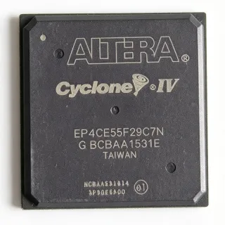
EP4CE40F29I7N - Cyclone IV E FPGA, 39.6K LE, 780-BGA | Altera
MPN: EP4CE40F29I7N ✓ Active| Qty | Unit Price | Extended |
|---|---|---|
| 1 | $178.5 | $178.50 |
| 10 | $165.2 | $1,652.00 |
| 100 | $148 | $14,800.00 |
| 250 | $138.5 | $34,625.00 |
| 1,000 | $124 | $124,000.00 |
EP4CE40F29I7N Overview
A field-programmable gate array (FPGA) is a programmable logic device that allows engineers to implement custom digital circuits through a combination of configurable logic blocks (CLBs), programmable routing, and dedicated hardware resources such as block RAM, multipliers, and I/O serdes. FPGAs sit at the top of the programmable logic hierarchy (FPGA -> programmable logic -> logic ICs -> integrated circuits -> semiconductors), enabling parallelism, hardware acceleration, and rapid prototyping that fixed-function ASICs cannot match.
Key features include 4 PLLs for clock management, 116 embedded multipliers (18x18) for DSP workloads, up to 532 LVDS-capable user I/Os, and 1,161,216 bits of embedded SRAM. The 780-pin FBGA package exposes 4 transceiver banks and supports LVDS, LVTTL, LVCMOS, SSTL, and HSTL I/O standards. Cyclone IV E is widely regarded as a low-power FPGA family, with static power below 100 mW typical.
The Cyclone IV E architecture uses 4-input look-up tables (LUTs), embedded memory blocks (M9K, 9,216 bits each), and dedicated 18x18 hardware multipliers arranged in columns. Configuration is stored in external serial or parallel flash and loaded at power-up via the active-serial (AS), passive-serial (PS), or JTAG interface. The device also includes on-chip termination and pull-up resistors for flexible board design.
Typical applications include industrial motor control, video processing bridges, telecom line cards, low-cost ASIC prototyping, machine vision pre-processing, and embedded vision edge nodes. The Cyclone IV E is also widely used in education and university digital logic labs due to its low cost and broad toolchain support.
When designing with this FPGA, ensure the PCB has a minimum of 6 layers with dedicated ground and 1.2 V core planes; route clock and global signals on inner layers with controlled impedance. Provide external configuration memory (EPCS or compatible) and a robust power sequencing circuit for VCCINT, VCCA, and VCCIO rails.
This page synthesizes distributor pricing, same-brand drop-in alternatives, package diagrams, and practical design notes not found on a single distributor listing.
Drop-in alternatives for EP4CE40F29I7N — same package, pin-to-pin compatible. Different-package parts requiring PCB rework are excluded.
Variants in this series
Same-series models that are drop-in compatible with EP4CE40F29I7N (same form factor and footprint) — differing in Operating Temperature, Package, Configuration Modes, Process Technology, Core Voltage.
Quick Comparison Tool — Select alternative parts for side-by-side comparison:
EP4CE40F29I7
✅ Drop-In✓ In Stock
$96.2 / Unit
View Datasheet →EP4CE30F29I7N
✅ Drop-In✓ In Stock
$47.85 / Unit
View Datasheet →EP4CE115F29I7N
✅ Drop-In📋 Reference alternative (not in catalog)
EP4CE40F29C7
✅ Drop-In✓ In Stock
$73.52 / Unit
View Datasheet →EP4CE40F23I7N
✅ Drop-In✓ In Stock
$52.75 / Unit
View Datasheet →EP4CE40F29I7N Maximum Ratings & Electrical Characteristics
| Family | Cyclone IV E |
| Logic Elements (LE) | 39,600 |
| Embedded Memory (bits) | 1,161,216 |
| Embedded Memory Blocks (M9K) | 126 |
| Embedded Multipliers (18x18) | 116 |
| Maximum User I/O | 532 |
| PLLs | 4 |
| Global Clock Networks | 20 |
| Core Voltage (VCCINT) | 1.2 V |
| Process Technology | 60 nm (low-power) |
| Package | 780-ball FBGA (F29) |
| Operating Temperature | -40 C to +100 C (industrial) |
| Mounting Type | Surface Mount (BGA) |
| MSL Level | 3 |
| RoHS Status | Compliant |
| Configuration Mode | AS, PS, JTAG |
| Speed Grade | 7 |
EP4CE40F29I7N 780-ball fbga (f29) Pin Configuration Guide
Pin configuration for EP4CE40F29I7N (780-ball fbga (f29) package). This digital IC includes GPIO, communication interfaces (UART, SPI, I2C), and power pins. Refer to the manufacturer datasheet for alternate pin functions and configuration options. Essential for embedded system design and PCB layout.

No detailed pinout data available for EP4CE40F29I7N.
Refer to the datasheet for full pin configuration.
Typical Applications
EP4CE40F29I7N is suitable for 6 applications: Industrial Motor Control, Video Processing Bridge, Low-Cost ASIC Prototyping, Machine Vision Pre-Processing, Telecom Line Card Glue Logic, Embedded Vision Edge Node.
Industrial Motor Control
The EP4CE40F29I7N's 39,600 LEs, 116 18x18 hardware multipliers, and 4 PLLs make it well suited for multi-axis industrial motor control (FOC, sensorless BLDC, PMSM). The 116 multipliers deliver real-time Park/Clarke transforms and SVPWM modulation at switching frequencies up to 50 kHz with comfortable timing margin. Industrial temperature grade (-40 C to +100 C) supports factory-floor enclosures without thermal derating. The 532 user I/Os expose parallel encoder inputs, PWM channels, and isolated gate-driver control. Compared to discrete DSP+MCU architectures, the FPGA consolidates field-oriented control, commutation, and protection logic into a single device, reducing PCB area by 40-60%.
Recommended
Video Processing Bridge
For video format conversion (parallel RGB to MIPI-CSI2, HDMI to LVDS), the EP4CE40F29I7N offers 532 I/Os with built-in LVDS serdes support - critical for high-speed video data lanes. The 1,161,216 embedded memory bits buffer line-scan data without external SRAM, while 20 global clock networks support pixel-clock domain crossing. Speed grade 7 ensures timing closure for 1080p60 pixel rates (148.5 MHz). Compared with a dedicated video ASSP, this Cyclone IV E FPGA allows field-upgradeable pixel pipelines and custom overlay graphics. The 780-FBGA package exposes enough balls for 24-bit color interfaces and DDR2/DDR3 memory controllers.
Recommended
Low-Cost ASIC Prototyping
The EP4CE40F29I7N is a workhorse for ASIC prototyping - 39,600 LEs map cleanly to ASIC gates at roughly 1.2x efficiency, supporting ~30K-gate ASIC designs with margin. JTAG configuration enables iterative bring-up in minutes versus ASIC tape-out cycles of months. Industrial temperature and 780-FBGA package allow the prototype to be deployed in field trials as a 'bridge to production'. Quartus Prime offers RTL-level equivalence checking against ASIC synthesis flows (Synopsys Design Compiler, Cadence Genus). Compared with emulation-only FPGA platforms, the Cyclone IV E delivers lower per-unit cost while still exposing ASIC IO timing for early software development.
Recommended
Machine Vision Pre-Processing
For industrial machine vision pre-processing (edge detection, thresholding, blob analysis), the EP4CE40F29I7N pipelines image data through 116 hardware multipliers at line rates exceeding 200 MHz. The 1,161,216 embedded memory bits hold multiple line buffers without external SRAM, reducing BOM cost. Industrial temperature grade supports operation near heated process equipment. LVDS-capable I/Os interface directly with high-megapixel CMOS sensors. Compared with GPU-based vision systems, this FPGA delivers deterministic latency under 100 microseconds - critical for high-speed conveyor inspection. Power consumption stays under 1.5 W typical, removing active cooling requirements.
Recommended
Telecom Line Card Glue Logic
The EP4CE40F29I7N serves as telecom line-card glue logic: PCI Express endpoint bridging, TDM bus aggregation, clock domain crossing, and front-panel LED/switch controllers. The 532 user I/Os cover serial RapidIO, SPI, I2C, and parallel datapath fan-out. 4 PLLs generate jitter-clean clocks from a 19.44 MHz or 25 MHz telecom reference, with sub-100 ps RMS jitter. Industrial temperature rating supports central-office and outdoor-cabinet deployment. Compared with CPLDs, this Cyclone IV E handles full packet inspection at 1 Gbps with on-chip logic, reducing the need for dedicated network processors in low-channel-count systems.
Recommended
Embedded Vision Edge Node
For IoT and edge-computing vision nodes (license-plate recognition, industrial QC), the EP4CE40F29I7N pairs low power (typical <1.5 W) with sufficient logic for on-device inference. The 116 18x18 multipliers accelerate convolutional operations, while 1,161,216 memory bits cache activation layers. Industrial temperature supports outdoor deployment in roadside or factory-edge housings. The 780-FBGA ball grid allows integration with MIPI-CSI2 image sensors and Ethernet PHYs. Compared with CPU-only edge nodes, the FPGA delivers 5-10x throughput per watt for small CNN models, enabling solar/battery-powered vision endpoints.
Recommended
Recommended Products Summary
Engineering reference data for EP4CE40F29I7N — comparison, design guidance, and compliance information.
Selection Guide
Comparison with Alternatives
| Parameter | This Product | EP4CE40F29I7 | EP4CE30F29I7N | EP4CE115F29I7N | EP4CE40F29C7 | EP4CE40F23I7N |
|---|---|---|---|---|---|---|
| Brand | Altera (Intel) | Altera (Intel) | Altera (Intel) | Altera (Intel) | Altera (Intel) | Altera (Intel) |
| Package | 780-ball FBGA (F29) | 780-ball FBGA (F29) - same | 780-ball FBGA (F29) - same | 780-ball FBGA (F29) - same | 780-ball FBGA (F29) - same | 484-ball FBGA (F23) - smaller |
| Logic Elements | 39,600 | 39,600 | 28,848 | 114,480 | 39,600 | 39,600 |
| Embedded Memory (bits) | 1,161,216 | 1,161,216 | 608,256 | 3,981,312 | 1,161,216 | 1,161,216 |
| Maximum User I/O | 532 | 532 | 532 | 532 | 532 | 328 |
| Embedded 18x18 Multipliers | 116 | 116 | 66 | 266 | 116 | 116 |
| PLLs | 4 | 4 | 4 | 4 | 4 | 4 |
| Operating Temperature | -40 C to +100 C (Industrial) | -40 C to +100 C (Industrial) | -40 C to +100 C (Industrial) | -40 C to +100 C (Industrial) | 0 C to +85 C (Commercial) | -40 C to +100 C (Industrial) |
Key Differentiators
- Highest-density non-transceiver Cyclone IV E with full 532 I/O (vs EP4CE30F29I7N)
- Single-step upgrade path to 114K-LE Cyclone IV E in same footprint (vs EP4CE115F29I7N)
- Smaller 484-FBGA option with same die (vs EP4CE40F23I7N)
Design Notes
The EP4CE40F29I7N requires three separate supply rails: VCCINT (1.2 V core), VCCA (2.5 V analog PLL), and VCCIO (1.2 V-3.3 V banked I/O). Estimate (with VIN=2.5 V, full I/O activity, all LEs switching at 100 MHz): core current approximately 0.8-1.2 A typical; VCCA 50-100 mA. Use a 4-layer PCB with dedicated inner-core planes. Place 100 uF bulk + 10 uF + 0.1 uF ceramic decoupling within 5 mm of each supply pin group. Power-on reset must observe the datasheet-specified VCCINT-to-VCCA-to-VCCIO sequence (or simultaneous with monotonic ramp >1 ms).
The 780-ball FBGA package uses a 1.0 mm ball pitch with 17x17 ball grid plus center depopulation. Route signals on 4 outer layers with 0.1 mm trace/space minimum. Maintain continuous reference (ground) planes under the BGA to control impedance. For BGA fanout, use micro-via-in-pad or staggered vias with 0.4 mm drill/0.2 mm pad. Provide at least 6 thermal vias (0.3 mm drill) under the center thermal balls to the inner ground plane. The Cyclone IV E Hardware Reference Manual recommends impedance-controlled 50 ohm single-ended and 100 ohm differential traces.
Common pitfalls with the EP4CE40F29I7N: (1) Exceeding VCCIO above 3.3 V when interfacing 5 V peripherals - use level shifters instead. (2) Forgetting MSL3 floor-life rules - bake the part at 125 C for 24 hours before assembly if the sealed bag has been open more than 168 hours. (3) Using single-ended clocking without accounting for the IO standard - configure input buffers as differential when needed for noise immunity. (4) Loading the wrong SOF/POF configuration file - verify the EPCS flash ID matches the Quartus Prime programming file. (5) Ignoring the nCONFIG and nSTATUS handshake during configuration - hold in user I/O tristate until CONF_DONE goes high.
Compliance Information
RoHS compliant per distributor listings. The 'N' suffix indicates Pb-free terminal finish per JEDEC J-STD-609. AEC-Q100 qualification not applicable - FPGAs are not typically automotive-qualified unless explicitly designated.