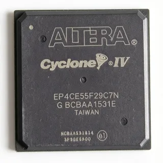
EP4CE75F29C9L - Cyclone IV E FPGA, 75K LEs, 780-BGA | Intel
MPN: EP4CE75F29C9L ✓ Active| Qty | Unit Price | Extended |
|---|---|---|
| 1 | $92.5 | $92.50 |
| 10 | $85.2 | $852.00 |
| 100 | $76 | $7,600.00 |
| 500 | $68.4 | $34,200.00 |
| 1,000 | $62.1 | $62,100.00 |
EP4CE75F29C9L Overview
A FPGA (Field-Programmable Gate Array) is a type of integrated circuit that can be reconfigured by the customer after manufacturing to implement custom digital logic functions. FPGAs occupy a tier above standard logic ICs and below ASICs in the semiconductor hierarchy: they provide ASIC-like parallelism and performance while retaining the flexibility and rapid development cycle of programmable logic. Cyclone IV E specifically targets low-power, high-volume designs where cost-per-logic-element and total power budget dominate the design trade-offs.
Key features include 4 PLLs (phase-locked loops) for flexible clock management, 426 embedded 18x18 hardware multipliers for DSP operations, 274 user I/O pins, support for external memory interfaces including DDR/DDR2 SDRAM and QDR II SRAM, and configuration via JTAG or active serial/parallel flash. The device operates from a 1.2V core supply with 1.2V/2.5V/3.3V multi-voltage I/O bank support, simplifying mixed-voltage system integration.
Architecturally, the Cyclone IV E family leverages a 4-input LUT-based logic fabric with distributed and block RAM, dedicated routing architecture with low skew, and embedded hard IP for memory controllers and high-speed transceivers are not present (transceivers belong to Cyclone IV GX). The 'F29' pin suffix denotes the 780-ball 1.0mm-pitch FBGA package, the 'C9' speed grade specifies a -8 commercial speed designation, and the 'L' suffix indicates a lead-free, RoHS-compliant finish.
Typical applications span industrial motor control, video processing pipelines, software-defined radio front-ends, low-cost ASIC prototyping, embedded vision systems, and portable test and measurement instruments where deterministic parallel processing and reconfigurability outweigh raw clock rate. For designs requiring a same-footprint upgrade path, the EP4CE115 family offers higher logic density while sharing the F29 780-BGA package.
A key design consideration is power planning: although Cyclone IV E is fabricated on a low-power process, designs that fully utilize all 75K logic elements with high toggle rates can exceed 3-5W total power. Designers should follow Intel's PowerPlay early power estimator and provide sufficient decoupling (typically 100nF + bulk capacitance per bank) plus a solid ground plane under the FBGA to control simultaneous switching noise. Without these precautions, the 1.0mm-pitch BGA is also challenging to rework in prototype runs.
Drop-in alternatives for EP4CE75F29C9L — same package, pin-to-pin compatible. Different-package parts requiring PCB rework are excluded.
Variants in this series
Same-series models that are drop-in compatible with EP4CE75F29C9L (same form factor and footprint) — differing in Operating Temperature, Package, Embedded 18x18 Multipliers, Process Technology, Speed Grade.
Quick Comparison Tool — Select alternative parts for side-by-side comparison:
EP4CE75F29C8N
✅ Drop-In✓ In Stock
$149.75 / Unit
View Datasheet →EP4CE75F29C8LN
✅ Drop-In✓ In Stock
$175.2 / Unit
View Datasheet →EP4CE75F29I7N
✅ Drop-In✓ In Stock
$540 / Unit
View Datasheet →EP4CE115F29C9L
✅ Drop-In📋 Reference alternative (not in catalog)
EP4CE115F29I7N
✅ Drop-In📋 Reference alternative (not in catalog)
EP4CE55F29C9L
✅ Drop-In✓ In Stock
$98.6 / Unit
View Datasheet →EP4CE75F29C9L Maximum Ratings & Electrical Characteristics
| Family | Cyclone IV E |
| Logic Elements | 75,408 |
| Logic Array Blocks (LABs) | 4,633 |
| Embedded Memory (bits) | 2,810,880 |
| M9K Memory Blocks | 305 |
| Embedded 18x18 Multipliers | 426 |
| PLLs | 4 |
| Global Clock Networks | 20 |
| Maximum User I/O Pins | 274 |
| Package | 780-ball FBGA (F29) |
| Pitch | 1.0 mm |
| Core Voltage | 1.2 V |
| Operating Temperature | 0C to +85C (commercial) |
| Speed Grade | C9 (commercial -8) |
| Process Technology | TSMC 60 nm low-power |
| Configuration Modes | JTAG, Active Serial, Active Parallel, Passive Serial |
| Lead-Free / RoHS | Yes (lead-free finish) |
EP4CE75F29C9L 780-ball fbga (f29) Pin Configuration Guide
Pin configuration for EP4CE75F29C9L (780-ball fbga (f29) package). This digital IC includes GPIO, communication interfaces (UART, SPI, I2C), and power pins. Refer to the manufacturer datasheet for alternate pin functions and configuration options. Essential for embedded system design and PCB layout.

No detailed pinout data available for EP4CE75F29C9L.
Refer to the datasheet for full pin configuration.
Typical Applications
EP4CE75F29C9L is suitable for 7 applications: Industrial Motor Control, Video Processing Pipeline, Software Defined Radio (SDR) Baseband, ASIC Prototyping and Emulation, Embedded Vision and Machine Vision, Portable Test and Measurement, LED Video Wall Driving.
Industrial Motor Control
The EP4CE75F29C9L fits industrial motor control with its 75,408 logic elements for state-machine and PID-loop implementations, plus 426 embedded 18x18 multipliers for Field-Oriented Control (FOC) math. The 4 PLLs generate precisely skewed PWM carriers while the 274 user I/Os interface directly to 3.3V gate drivers without level shifters. Designers achieve closed-loop torque response below 10us by parallelizing Clarke/Park transforms in dedicated multiplier columns rather than soft cores. The 780-BGA's solid GND plane also reduces switching noise in 10-30kHz PWM environments.
Recommended
Video Processing Pipeline
The EP4CE75F29C9L's 2,810,880 bits of embedded memory (305 M9K blocks) provide sufficient line buffering for 720p/1080p video at 60fps in single-channel designs or 480p in dual-channel configurations. The 426 hardware multipliers accelerate 2D filter kernels, scaling operations, and Bayer demosaic without consuming soft multiplier resources. Multi-voltage I/O banks interface directly to BT.656, BT.1120, and MIPI-CSI2 bridges, eliminating external voltage translators. The 60nm low-power process keeps video frame-grabber board power under 3-4W versus competing FPGAs at higher process nodes.
Recommended
Software Defined Radio (SDR) Baseband
In SDR baseband processing, the EP4CE75F29C9L's 426 18x18 multipliers implement up to 100-tap FIR filters and FFT butterflies running at 200+ MHz sample rate. The 4 PLLs derive orthogonal LO synthesis from a single reference, and 274 user I/Os route digitized IQ streams to DACs/ADCs. Designers favor this Cyclone IV E part over Cyclone IV GX for cost-sensitive narrowband (<30 MHz) commercial radios where transceivers are not required. Pin-compatible migration to EP4CE115F29C9L allows scaling to wideband multi-channel designs.
Recommended
ASIC Prototyping and Emulation
The EP4CE75F29C9L provides 75,408 logic elements for prototyping mid-complexity ASIC RTL prior to tape-out, with timing-accurate synthesis supported through Intel Quartus Prime. The 305 M9K blocks serve as register-file and cache emulators, while 426 multipliers handle DSP block behavioral equivalents. Engineers split large ASIC designs across multiple FPGAs using the 274 user I/Os as chip-to-chip links, achieving MHz-class validation. The 780-BGA's 1.0mm pitch also enables cost-effective multi-FPGA daughter cards versus finer-pitch BGA prototyping platforms.
Recommended
Embedded Vision and Machine Vision
For machine vision, the EP4CE75F29C9L implements Sobel/Canny edge detection, color-space conversion, and Hough transforms entirely in hardware, leveraging its 426 multipliers for matrix multiplications on feature vectors. The 2,810,880 embedded RAM bits buffer raw Bayer/YCbCr frames for pipelined processing without external SRAM in lower-resolution sensors (<2MP). The 20 global clock networks enable independent domains for sensor ingress, processing, and host-side egress. At a 2026-09-10 unit price around $92.50, the part achieves cost targets for volume industrial-camera deployments.
Recommended
Portable Test and Measurement
The EP4CE75F29C9L's 60nm low-power process delivers logic density at power budgets compatible with portable oscilloscopes, logic analyzers, and bench-top protocol testers. The 4 PLLs synthesize arbitrary sample clocks from a low-cost crystal, and 426 hardware multipliers accelerate FFT-based spectrum analysis. 274 user I/Os accommodate high-channel-count logic-analyzer probes (32-64 channels) plus display and USB interface. Pin-compatible EP4CE115F29C9L enables product-line scaling for higher-end models without PCB redesign.
Recommended
LED Video Wall Driving
The EP4CE75F29C9L's 75,408 logic elements and 426 hardware multipliers suit LED video wall scan-line generation and gamma correction across multiple panel chains. The 274 user I/Os drive hundreds of parallel LED data lines directly, eliminating costly serializer/deserializer (SerDes) parts. The 2,810,880 bits of embedded memory absorb frame-buffer slices for color-space conversion and refresh-rate adjustment. Compared to microcontrollers, this FPGA achieves the deterministic multi-MHz pixel rate required for smooth 4K video walls.
Recommended
Recommended Products Summary
Engineering reference data for EP4CE75F29C9L — comparison, design guidance, and compliance information.
Selection Guide
Comparison with Alternatives
| Parameter | This Product | EP4CE75F29C8N | EP4CE75F29I7N | EP4CE115F29C9L | EP4CE55F29C9L |
|---|---|---|---|---|---|
| Package | 780-ball FBGA (F29), 1.0mm pitch | 780-ball FBGA (F29), 1.0mm pitch - same | 780-ball FBGA (F29), 1.0mm pitch - same | 780-ball FBGA (F29), 1.0mm pitch - same | 780-ball FBGA (F29), 1.0mm pitch - same |
| Brand | Intel (formerly Altera) | Intel | Intel | Intel | Intel |
| Logic Elements | 75,408 | 75,408 (identical) | 75,408 (identical) | 114,480 (+52%) | 55,408 (-27%) |
| Embedded Memory (bits) | 2,810,880 | 2,810,880 (identical) | 2,810,880 (identical) | 3,981,312 (+42%) | 2,109,696 (-25%) |
| 18x18 Multipliers | 426 | 426 (identical) | 426 (identical) | 532 (+25%) | 312 (-27%) |
| PLLs | 4 | 4 (identical) | 4 (identical) | 4 (identical) | 4 (identical) |
| Max User I/O | 274 | 274 (identical) | 274 (identical) | 274 (identical) | 274 (identical) |
| Speed Grade | C9 (commercial -8) | C8 (commercial, slower) | I7 (industrial) | C9 (same) | C9 (same) |
| Temperature Grade | Commercial 0C to +85C | Commercial 0C to +85C | Industrial -40C to +100C | Commercial 0C to +85C | Commercial 0C to +85C |
Key Differentiators
- Pin-compatible logic density upgrade path (vs EP4CE55F29C9L)
- Industry-standard 60nm low-power process (vs EP4CE115F29C9L)
- Commercial speed-grade cost optimization (vs EP4CE75F29I7N)
- 274 user I/O count on F29 package (vs Smaller F23 packages in same family)
Design Notes
Use the Intel PowerPlay Early Power Estimator before schematic capture to size the 1.2V VCCINT regulator and decouple rails. A 75K-LE Cyclone IV E at high toggle rate can draw 2-4A transient on VCCINT; place 100nF ceramic caps on every VCCINT pin and bulk 47-100uF polymer near the package. VCCIO must be supplied for every bank in use, including unused banks set to a known voltage to avoid floating-pin leakage.
Estimated: at ~3W total power with the FBGA-780 substrate and 0C-85C ambient, junction temperature rise is approximately 25C on a 4-layer 1oz PCB with thermal vias under the central BGA balls. For fanless enclosures, derate system ambient below 60C or migrate to EP4CE55F29 with similar package. Always verify with the PowerPlay Thermal Power Output in actual post-place-and-route data.
The 1.0mm-pitch 780-ball FBGA requires 4-layer (preferably 6-layer) PCB with laser-drilled or micro-via fanout for the center ball rows. Use 0.4mm via pads with 0.2mm drill for inner rows, and ensure solder mask defined (SMD) pads rather than non-solder mask defined (NSMD) for higher assembly yield. Plan a solid GND plane directly under the BGA to control simultaneous switching noise on multi-MHz I/O banks.
Group high-speed differential pairs (LVDS) within a single I/O bank to minimize reference-clock skew and pin-out complications. Route DDR2/DDR3 address/command signals with matched trace lengths (within +/-25 mil of byte-lane group) and 100-ohm differential impedance. Keep PLL analog supply pins filtered with ferrite beads and isolated digital-side noise to within 25 mils of ground.
Do not leave configuration MSEL[3:0] pins floating - they select the configuration scheme (AS, AP, PS, JTAG) and must be tied high/low per datasheet. JTAG TCK frequency must be 3-4x slower than the slowest device in the chain if programming multiple FPGAs in series. Finally, never hot-plug the EP4CE75F29C9L; always ramp core power monotonically to avoid latch-up on the 60nm CMOS process.
Compliance Information
L suffix in C9L denotes lead-free matte tin plating compliant with RoHS. Cyclone IV E family not AEC-Q100 qualified; for automotive ASIL applications choose Cyclone V or later families.