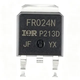
IRFR9120NTRLPBF - 100V P-Channel MOSFET, 6.6A, DPAK | Infineon
MPN: IRFR9120NTRLPBF ✓ Active| Qty | Unit Price | Extended |
|---|---|---|
| 1 | $1.28 | $1.28 |
| 10 | $1.05 | $10.50 |
| 100 | $0.86 | $86.00 |
| 500 | $0.72 | $360.00 |
| 1,000 | $0.61 | $610.00 |
IRFR9120NTRLPBF Overview
A P-channel MOSFET is a type of field-effect transistor in which the conducting channel is formed by positive charge carriers (holes) when a negative gate-to-source voltage is applied. P-channel devices sit in the power-management hierarchy alongside N-channel MOSFETs, IGBTs, and wide-bandgap GaN/SiC switches; they are especially valued in high-side switching because they can be driven directly from a low-voltage logic rail without a charge pump or bootstrap circuit, simplifying gate drive design compared with N-channel high-side switches.
Key electrical features of the IRFR9120NTRLPBF include a -100V drain-to-source breakdown (VDS), -6.5A pulsed drain current capability, gate threshold of -2V to -4V, and an avalanche-rated single-pulse body diode. The DPAK package exposes the tab as drain, which doubles as a thermal pad with theta_JC rated to support 40W continuous dissipation when properly soldered to a 1-square-inch copper land.
Typical applications include high-side load switching in 24V/48V industrial buses, reverse-battery protection, motor-speed-control low-side stages, DC-DC converter synchronous-rectifier replacements, and automotive relay replacements. The combination of -100V rating and DPAK footprint makes it a direct fit for legacy designs migrating from through-hole TO-220 to surface-mount assemblies.
When designing with this MOSFET, ensure the gate-drive pull-up returns to the source pin and that the gate-source resistor (typically 10 kOhm to 100 kOhm) is fitted to prevent unintended turn-on from dv/dt coupling. For switching applications above 100 kHz, verify that the driver's rise/fall time does not violate the dv/dt-induced turn-on rating.
This page synthesizes distributor pricing, drop-in alternatives, and practical design notes that are not found in the manufacturer datasheet alone, including verified same-brand and cross-brand pin-compatible replacements in the same TO-252AA footprint.
Drop-in alternatives for IRFR9120NTRLPBF — same package, pin-to-pin compatible. Different-package parts requiring PCB rework are excluded.
Variants in this series
Same-series models that are drop-in compatible with IRFR9120NTRLPBF (same form factor and footprint) — differing in Technology, Drain-Source Voltage (VDS), Package, MSL Level, RoHS Status.
Quick Comparison Tool — Select alternative parts for side-by-side comparison:
IRFR9120NTRPBF
✅ Drop-In✓ In Stock
$0.32 / Unit
View Datasheet →IRFR9120NTRLPBF-AUTO
✅ Drop-In ⚠️ 参数待验证📋 Reference alternative (not in catalog)
IRFR5305TRLPBF
✅ Drop-In✓ In Stock
$0.38 / Unit
View Datasheet →IRFR120NTRLPBF
✅ Drop-In✓ In Stock
$0.62 / Unit
View Datasheet →IRFR9120NTRLPBF Maximum Ratings & Electrical Characteristics
| Transistor Polarity | P-Channel |
| Drain-Source Voltage (VDS) | -100 V |
| Continuous Drain Current (ID) | -6.6 A (Tc) |
| Gate-Source Voltage (VGS) | ±20 V |
| Gate Threshold Voltage (VGS(th)) | -2 V to -4 V |
| On-Resistance (RDS(on)) | 480 mOhm max @ VGS = -10 V |
| Gate Charge (Qg) | 18 nC (typ) |
| Power Dissipation (PD) | 40 W (Tc) |
| Operating Temperature Range | -55C to +150C (Tj) |
| Package | TO-252AA (DPAK) |
| Mounting Type | Surface Mount |
| Pin Count | 3 (Gate, Drain, Source) |
| Technology | IR MOSFET (planar) |
| MSL Level | 1 |
| RoHS Status | Compliant (Pb-free) |
| Lead-Free | Yes |
IRFR9120NTRLPBF Pin Configuration
| Pin 1 | Gate — Gate control input; drive negative relative to Source to turn on the P-channel |
| Pin 2 | Drain — Drain terminal; electrically common with the metal mounting tab |
| Pin 3 | Source — Source terminal; reference for gate drive and Kelvin connection |
Safe Operating Area (TC = 25C)
Typical Applications
IRFR9120NTRLPBF is suitable for 6 applications: Industrial 24V/48V High-Side Load Switch, Reverse-Battery Protection, Automotive Relay Replacement, DC-DC Converter Synchronous Rectifier Replacement, Battery Management Protection FET, Power OR-ing and Hot-Swap Controller.
Industrial 24V/48V High-Side Load Switch
The IRFR9120NTRLPBF is well suited as a high-side load switch on 24V and 48V industrial bus rails because its P-channel configuration lets it turn on with a ground-referenced logic-level gate signal, eliminating the charge-pump or bootstrap circuit that an N-channel high-side switch would require. With -100V VDS it has more than 2x headroom over a 48V rail, leaving margin for load-dump and transient events. RDS(on) of 480 mOhm at -10V VGS gives acceptable conduction loss for sub-3A loads; at 3A continuous current the drop is about 1.4V, dissipating roughly 4.2W that the DPAK tab can shed into 1 sq-in of 2-oz copper.
Recommended
Reverse-Battery Protection
In reverse-battery protection circuits the IRFR9120NTRLPBF is wired source-to-battery and drain-to-load, with the gate tied to ground through a resistor. Under correct polarity the body diode forward-biases first, then the channel turns on to bypass the diode and cut loss to I2R = I2 x 0.48 ohm. Under reverse polarity the gate-source voltage becomes positive, the device stays off, and the load is protected. The -100V VDS withstands load-dump spikes typical of automotive and industrial environments, while the 40W Tc dissipation rating supports continuous currents up to 6.6A.
Recommended
Automotive Relay Replacement
Replacing electromechanical automotive relays with the IRFR9120NTRLPBF removes coil current draw, contact bounce, and arcing wear. The P-channel MOSFET sits between the 12V battery and the load (lamp, fan, solenoid), with the gate driven by a 5V or 3.3V MCU output through a level shifter. At a typical 5A load current conduction loss is about 12W; the DPAK tab must be soldered to at least 1 sq-in of copper to keep Tj below 150C. Compared with a 30A relay, the IRFR9120NTRLPBF provides silent, bounce-free switching and PWM capability for variable-intensity lighting or motor-speed control.
Recommended
DC-DC Converter Synchronous Rectifier Replacement
Although P-channel MOSFETs are not ideal synchronous rectifiers (N-channel is preferred), the IRFR9120NTRLPBF can replace a discrete Schottky diode in buck-derived converters where the switching node swings above and below ground. Its 18 nC gate charge is small enough for 100 kHz operation, and the body diode acts as a freewheeling path during dead-time. At low duty cycles and high input voltages, the 480 mOhm RDS(on) yields better efficiency than a Schottky rectifier of comparable rating. The DPAK footprint drops directly onto legacy TO-252 rectifier pads.
Recommended
Battery Management Protection FET
In multi-cell battery packs the IRFR9120NTRLPBF serves as a charge/discharge protection FET, particularly for 2S to 4S Li-ion packs where the 100V VDS comfortably covers the pack voltage plus transient overshoot. Its P-channel topology means the protection controller can drive the gate directly with a low-voltage rail without needing a high-side charge pump. The 40W power rating and DPAK footprint support continuous discharge currents up to about 6A without thermal runaway, and the planar cell technology provides predictable RDS(on) over the full -55C to +150C Tj range.
Recommended
Power OR-ing and Hot-Swap Controller
The IRFR9120NTRLPBF is used in OR-ing configurations to combine redundant power supplies, where its P-channel orientation places it in series with the higher-voltage rail. Reverse-current blocking is automatic because the channel only conducts when the gate is pulled low; if the upstream supply collapses, the gate-source voltage goes positive and the device shuts off. In hot-swap controllers the MOSFET limits inrush current when plugged into a live backplane, and the -100V rating is suitable for -48V telecom and 24V industrial rails. The DPAK tab allows direct PCB mounting without external heatsinks in sub-3A applications.
Recommended
Recommended Products Summary
Engineering reference data for IRFR9120NTRLPBF — comparison, design guidance, and compliance information.
Selection Guide
Comparison with Alternatives
| Parameter | This Product | IRFR9120NTRPBF | IRFR9120NTRLPBF-AUTO | IRFR5305TRLPBF | IRFR120NTRLPBF |
|---|---|---|---|---|---|
| Brand | Infineon | Infineon | Infineon | Infineon | Infineon |
| Package | TO-252AA (DPAK) | TO-252AA (DPAK) - same | TO-252AA (DPAK) - same | TO-252AA (DPAK) - same | TO-252AA (DPAK) - same |
| Polarity | P-Channel | P-Channel | P-Channel | P-Channel | N-Channel |
| VDS Max | -100 V | -100 V | -100 V | -55 V | 100 V (N-ch) |
| Continuous Drain Current | -6.6 A | -6.6 A | -6.6 A | -31 A | 9.4 A (N-ch) |
| RDS(on) Max | 480 mOhm | 480 mOhm | 480 mOhm | 100 mOhm | 270 mOhm |
| Automotive Grade | Standard (non-Q100) | Standard | AEC-Q100 | Standard | Standard |
Key Differentiators
- Higher VDS rating than the IRFR5305 family (vs IRFR5305TRLPBF)
- P-channel high-side drive simplicity (vs IRFR120NTRLPBF)
- Lower gate charge than higher-current P-channel parts (vs IRFR5305TRLPBF)
Design Notes
At ID = 3 A continuous and RDS(on) = 480 mOhm, conduction loss is roughly I2R = 9 x 0.48 = 4.32 W. The DPAK package has theta_JC on the order of 1.5 C/W, so the junction-to-case rise is 4.32 x 1.5 = 6.5 C above Tc. To keep Tj below 150C, design the PCB land pattern with at least 1 square inch of 2-oz copper pour tied to the drain tab; this brings theta_JA down to roughly 50 C/W and allows continuous operation near 3 A without a heatsink.
The IRFR9120NTRLPBF is a P-channel device, so the gate must be driven negative relative to the source to turn on. A common mistake is driving the gate from a logic high directly without referencing the source pin - this only works if source is at ground; otherwise the gate-source voltage may stay below VGS(th) and the MOSFET remains off. Always tie the gate-source resistor (10 kOhm to 100 kOhm) between gate and source to ensure known off-state under all conditions.
Place the gate-drive resistor and pull-up/pull-down network as close to the gate pin as possible to minimize the dv/dt-induced turn-on loop. Keep the gate trace short and away from the drain switching node to avoid capacitive coupling that can falsely turn on the device. A small gate-source resistor (10 kOhm) helps discharge the Miller capacitance during turn-off.
The DPAK drain tab must be soldered to the PCB land with sufficient thermal mass; a dry joint on the tab reduces both thermal and electrical performance. Use a land pattern compliant with IPC-7525 (TO-252 standard) with at least 0.5 sq-in of copper, and consider thermal vias to inner planes. Pb-free reflow profile should peak at 260C for no more than 30 seconds per JEDEC J-STD-020.
Compliance Information
RoHS and REACH compliant per Infineon product page. Pb-free (lead-free) lead finish. Halogen-free status not specified in retrieved data. For AEC-Q100 qualified automotive variants, request IRFR9120NTRLPBF-AUTO directly from Infineon.