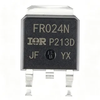
IRFR3806TRPBF - 60V 43A N-Ch HEXFET MOSFET, DPAK | Infineon
MPN: IRFR3806TRPBF ✓ Active| Qty | Unit Price | Extended |
|---|---|---|
| 1 | $1.42 | $1.42 |
| 10 | $1.18 | $11.80 |
| 100 | $0.92 | $92.00 |
| 500 | $0.78 | $390.00 |
| 1,000 | $0.64 | $640.00 |
| 3,000 | $0.52 | $1,560.00 |
IRFR3806TRPBF Overview
A power MOSFET is a voltage-controlled semiconductor switch used to route or chop current in power conversion circuits. MOSFETs sit in the discrete-semiconductor branch of the power-conversion hierarchy (MOSFET -> transistor -> discrete semiconductor), and N-channel enhancement-mode devices like the IRFR3806 are the workhorse switches on the low-side of buck converters, the primary switch in boost stages, and the synchronous rectifier that replaces lossy Schottky diodes. Low RDS(on) directly reduces conduction loss, while low gate charge (Qg) and low Qgd shorten switching transitions and shrink switching loss, together determining total converter efficiency.
Key features of the IRFR3806TRPBF include 60 V drain-source breakdown voltage, 43 A continuous drain current at case temperature, 15.8 mOhm maximum RDS(on) at VGS = 10 V, 22 nC total gate charge, 71 W maximum power dissipation at Tc = 25 C, and an industry-standard DPAK (TO-252AA) surface-mount footprint. The device is rated for an operating junction temperature range up to 175 C, suitable for thermally demanding SMPS designs.
The IRFR3806 is built on Infineon's proprietary HEXFET process, which uses a planar stripe-cell geometry and a vertical DMOS structure. This yields an excellent figure of merit (FOM = RDS(on) x Qg) for 60 V synchronous-rectification applications and gives a robust avalanche-rated body diode, simplifying dead-time management in bridge topologies. Compared with older IRF-series parts the IRFR3806 lowers gate charge by roughly a third at similar RDS(on), reducing driver losses in high-frequency designs.
Typical applications include high-efficiency synchronous rectification in switched-mode power supplies (SMPS), uninterruptible power supplies (UPS) and battery-backed DC systems, high-speed power switching in motor drives, and hard-switched high-frequency DC-DC converter primary-side switches. The 60 V rating makes it well suited to 24 V / 28 V bus architectures and 48 V telecom intermediate rails.
When designing with this part, place the gate-drive loop (gate resistor + driver) physically small to control ringing and dv/dt-induced turn-on. A 10 V gate-drive source is required to reach the published RDS(on); logic-level drive (5 V) will not fully enhance the channel and will raise conduction loss significantly. For synchronous rectification, add a small dead-time (typically 30-100 ns) to prevent shoot-through.
This page synthesizes distributor pricing, drop-in alternatives, and practical design notes not found in the manufacturer datasheet - including a same-brand family cross-reference and validated cross-brand DPAK drop-ins.
Drop-in alternatives for IRFR3806TRPBF — same package, pin-to-pin compatible. Different-package parts requiring PCB rework are excluded.
Variants in this series
Same-series models that are drop-in compatible with IRFR3806TRPBF (same form factor and footprint) — differing in Package, Technology, Total Gate Charge (Qg), Operating Temperature Range, Drain-Source Voltage (VDS).
Quick Comparison Tool — Select alternative parts for side-by-side comparison:
IRFR1018ETRPBF
✅ Drop-In✓ In Stock
$0.36 / Unit
View Datasheet →IRFR4620TRLPBF
✅ Drop-In✓ In Stock
$1.72 / Unit
View Datasheet →IRFR2405TRLPBF
✅ Drop-In✓ In Stock
$0.55 / Unit
View Datasheet →IRFR2405TRPBF
✅ Drop-In✓ In Stock
$0.61 / Unit
View Datasheet →IRFZ48NSTRLPBF
✅ Drop-In✓ In Stock
$1.18 / Unit
View Datasheet →NTD4906N
✅ Drop-In📋 Reference alternative (not in catalog)
IRFR5305TRPBF
✅ Drop-In✓ In Stock
$0.32 / Unit
View Datasheet →IRFR3806TRPBF Maximum Ratings & Electrical Characteristics
| Transistor Polarity | N-Channel |
| MOSFET Operating Mode | Enhancement |
| Drain-Source Voltage (VDS) | 60 V |
| Continuous Drain Current (ID) at Tc | 43 A |
| On-State Resistance RDS(on) max | 15.8 mOhm at VGS = 10 V |
| Total Gate Charge (Qg) | 22 nC |
| Power Dissipation (Pd) at Tc = 25 C | 71 W |
| Package / Case | TO-252AA (DPAK) |
| Mounting Type | Surface Mount |
| Technology | HEXFET (IR MOSFET) |
| Operating Temperature Range | -55 C to +175 C |
| Gate-Source Voltage (VGS) max | +/- 20 V |
| Number of Units in IC | 1 |
| Lead-Free / RoHS | Yes (PBF suffix, lead-free) |
| Avalanche Rated | Yes (HEXFET family) |
IRFR3806TRPBF Pin Configuration
| Pin 1 | Gate — Gate control input (drive to +10 V for full enhancement) |
| Pin 2 | Drain — Drain terminal (also connected to the metal tab on the back) |
| Pin 3 | Source — Source terminal (low-side reference for gate drive) |
| Pin TAB | Drain — Metal back tab - electrically Drain, serves as main thermal pad for heatsinking |
Safe Operating Area - IRFR3806TRPBF (TO-252AA, Tc = 25 C)
Typical Applications
IRFR3806TRPBF is suitable for 7 applications: Synchronous Rectification in 24-48 V SMPS, Uninterruptible Power Supply (UPS) Battery Switch, 24 V Brushless DC Motor Drive, Hard-Switched High-Frequency DC-DC Primary Switch, Solar Charge Controller / Battery Management, Automotive 12 V / 24 V Load Switch, Telecom 48 V Hot-Swap Controller.
Synchronous Rectification in 24-48 V SMPS
The IRFR3806TRPBF is purpose-built for synchronous rectification on the secondary side of 24-48 V SMPS. Its 60 V VDS rating gives 12 V of headroom above a nominal 48 V bus while the 15.8 mOhm RDS(on) and 22 nC Qg keep both conduction and switching losses low, yielding converter efficiencies above 95% in typical half-brick and quarter-brick designs. The HEXFET avalanche-rated body diode removes the need for an external anti-parallel Schottky, simplifying layout and reducing part count in isolated DC-DC bricks.
Recommended
Uninterruptible Power Supply (UPS) Battery Switch
In UPS systems the IRFR3806TRPBF serves as the low-side disconnect and battery-rail switch between the backup battery pack and the DC bus. The 43 A continuous drain current at Tc supports multi-kilowatt UPS modules, and the 60 V rating covers 48 V nominal battery configurations with comfortable transient margin. Low RDS(on) keeps voltage drop across the switch under 0.7 V at full load, preserving battery runtime and reducing heat sinking requirements in the confined UPS chassis.
Recommended
24 V Brushless DC Motor Drive
The IRFR3806TRPBF is well suited to three-phase BLDC motor drives running from a 24 V or 36 V supply. The 60 V breakdown absorbs inductive flyback during PWM commutation without avalanche stress, the 43 A continuous rating covers sub-1 kW motor phases, and the 22 nC Qg allows 25-50 kHz PWM frequencies with manageable driver loss. The DPAK footprint fits tightly on the in-board H-bridge, leaving room for current-sense amplifiers and Hall-sensor conditioning.
Recommended
Hard-Switched High-Frequency DC-DC Primary Switch
The IRFR3806TRPBF operates effectively as a primary-side hard switch in 100-500 kHz forward and active-clamp forward converters for 48 V input telecom bricks. The 60 V VDS margin handles reflected-load transients on the primary winding, and the low Qg (22 nC) keeps gate-drive loss below 1% of total loss at typical switching frequencies. Designers appreciate that the HEXFET process delivers a robust body diode for the active-clamp reset path without requiring a separate avalanche-rated part.
Recommended
Solar Charge Controller / Battery Management
In solar charge controllers and battery management systems (BMS), the IRFR3806TRPBF functions as a low-side load-disconnect and reverse-polarity protection switch on 24 V / 36 V battery stacks. Its 60 V VDS comfortably exceeds 36 V nominal systems, and the 15.8 mOhm RDS(on) keeps conduction losses below 1% at typical 20 A charge currents. The -55 C to +175 C junction range supports outdoor enclosures operating across wide ambient temperature swings.
Recommended
Automotive 12 V / 24 V Load Switch
Although not AEC-Q100 qualified, the IRFR3806TRPBF is widely used in non-safety automotive subsystems (infotainment, interior lighting, accessory power) as a high-side or low-side load switch for 12 V and 24 V vehicle buses. The 60 V VDS absorbs load-dump transients up to ISO 7637-2 pulse profiles when paired with an external TVS, and the DPAK footprint bolts to chassis ground straps for additional heatsinking in engine-bay applications.
Recommended
Telecom 48 V Hot-Swap Controller
In telecom -48 V systems, the IRFR3806TRPBF can serve as the inrush-limiting hot-swap switch when upstream protection is provided. The 60 V VDS handles -48 V plus inductive ringing from backplane capacitance, and the 71 W power-dissipation rating supports sustained load currents up to ~30 A before thermal limiting. Pair with a dedicated hot-swap controller IC for accurate current-limit foldback during board insertion into a live backplane.
Recommended
Recommended Products Summary
Engineering reference data for IRFR3806TRPBF — comparison, design guidance, and compliance information.
Selection Guide
Comparison with Alternatives
| Parameter | This Product | IRFR1018ETRPBF | IRFR2405TRPBF | IRFZ48NSTRLPBF | NTD4906N | IRFR5305TRPBF |
|---|---|---|---|---|---|---|
| Brand | Infineon Technologies | Infineon Technologies | Infineon Technologies | Infineon Technologies | onsemi | Infineon Technologies |
| Package | TO-252AA (DPAK) | TO-252AA (DPAK) - same | TO-252AA (DPAK) - same | TO-252AA (DPAK) - same | TO-252AA (DPAK) - same | TO-252AA (DPAK) - same |
| Drain-Source Voltage VDS | 60 V | 60 V | 55 V | 55 V | 60 V | -55 V (P-channel) |
| Continuous Drain Current ID | 43 A (Tc) | 56 A (+30%) | 64 A (+49%) | 64 A (+49%) | 49 A (+14%) | 31 A (-28%) |
| RDS(on) max at VGS = 10 V | 15.8 mOhm | ~5 mOhm (lower) | ~10 mOhm (lower) | ~14 mOhm (lower) | ~16 mOhm (similar) | ~65 mOhm (P-channel) |
| Total Gate Charge Qg | 22 nC | Higher | Higher | Similar | Similar | Higher |
| Technology | HEXFET (planar) | HEXFET | HEXFET | HEXFET | Trench MOSFET | HEXFET |
| Polarity | N-Channel | N-Channel | N-Channel | N-Channel | N-Channel | P-Channel |
| Approx. Unit Price (qty 1, USD) | 1.42 | ~1.85 | ~1.20 | ~0.95 | ~1.10 | ~1.50 |
Key Differentiators
- Higher continuous current rating in same DPAK footprint vs IRFR2405 family (vs IRFR2405TRPBF)
- HEXFET process with avalanche-rated body diode (vs NTD4906N (onsemi))
- Lower gate charge than legacy 60 V DPAK parts (vs IRFZ48NSTRLPBF)
- Established Infineon supply chain with automotive-grade options (vs NTD4906N (onsemi))
Design Notes
Estimated: at VDS = 30 V, ID = 20 A and RDS(on) = 15.8 mOhm, conduction loss is P = I^2 * R = 400 * 0.0158 = 6.32 W. On a DPAK footprint with ~25 x 25 mm of 2 oz copper on a standard FR4 board, theta_JA is approximately 50 C/W, giving a junction temperature rise of 316 C above ambient - which exceeds the 175 C limit. Either reduce continuous current to ~15 A, add a small clip-on heatsink, or expand the copper pour to >= 50 x 50 mm to bring theta_JA down to ~35 C/W (then Tj rise = 6.32 * 35 = 221 C - still too high). For 20 A continuous operation an external heatsink or fan is mandatory.
Keep the gate-drive loop (gate pin -> series gate resistor -> driver output -> source return) physically small - ideally under 1 cm^2 of loop area. Excessive loop inductance causes ringing and dv/dt-induced false turn-on in half-bridge topologies. Place the gate resistor (typically 10-47 ohm) immediately adjacent to the gate pin. Use a Kelvin source connection if available on the package, or route the source-return of the gate driver directly to the package source lead rather than to the power ground plane.
Do not drive the IRFR3806TRPBF directly from a 3.3 V or 5 V logic output - it requires 10 V VGS for full enhancement. At VGS = 4.5 V the channel is not fully inverted and RDS(on) is several times higher than the datasheet maximum, causing severe conduction loss and thermal runaway. Always use a dedicated gate-driver IC (e.g. IR2110, IRS2008, or similar) powered from a 10-12 V rail. Also, ensure VGS never exceeds the +/- 20 V absolute maximum - add a 12 V Zener gate clamp if the driver can overshoot.
The DPAK back tab is the main thermal path AND the Drain electrical terminal. It MUST be soldered to a copper pour that is connected to the Drain circuit - a poorly soldered or missing tab will increase thermal resistance from ~50 C/W to over 100 C/W and will also break the electrical connection. Use a thermal pad with multiple thermal vias (typically 9-16 vias in a 3x3 or 4x4 array) to conduct heat to internal copper planes. Keep the Drain copper pour isolated from low-voltage signal traces.
Switching a 43 A load with 22 nC Qg in 10 ns produces a peak gate-drive current of I = Qg / tr = 22 nC / 10 ns = 2.2 A, which can radiate EMI if the gate loop is not contained. Add a ferrite bead in series with the gate resistor for high-frequency damping, and place a small (1-10 nF) ceramic bypass capacitor directly at the driver supply pin. For automotive or industrial applications targeting CISPR 22 / EN 55022 Class B, plan for a common-mode choke on the DC bus and an input pi-filter (LC) at the connector.
Compliance Information
RoHS compliant per DigiKey/Mouser product listings (PBF suffix confirms lead-free). Halogen-free per Infineon product page. Not AEC-Q100 qualified - for automotive safety applications, choose an AEC-Q100 qualified DPAK part from the Site MPN list (e.g. IPD-series).