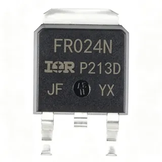
IRLR2705TRPBF - 55V 28A N-Channel HEXFET MOSFET | Infineon
MPN: IRLR2705TRPBF ✓ Active| Qty | Unit Price | Extended |
|---|---|---|
| 1 | $0.92 | $0.92 |
| 10 | $0.78 | $7.80 |
| 100 | $0.62 | $62.00 |
| 500 | $0.51 | $255.00 |
| 1,000 | $0.43 | $430.00 |
| 2,500 | $0.36 | $900.00 |
IRLR2705TRPBF Overview
A power MOSFET is a voltage-controlled semiconductor switch used to efficiently route or modulate current in DC-DC converters, motor drives, load switches, and battery protection circuits. Within the broader taxonomy, the IRLR2705TRPBF sits in the N-channel enhancement-mode MOSFET family, which is the dominant topology for low-side switching because electrons (the majority carrier) deliver 2-3x lower on-resistance per unit area than P-channel equivalents. N-channel MOSFETs in DPAK packages remain the workhorse of 12V/24V automotive, industrial, and consumer power designs.
Key features of the IRLR2705TRPBF include logic-level VGS(th) compatible with 4V drive, fast switching speed (Qg = 16.7 nC typical per Mouser listing), 68W maximum power dissipation at Tc, and an intrinsic body diode rated for avalanche energy. The DPAK (TO-252AA) footprint offers a thermally efficient exposed pad that delivers roughly 50 C/W junction-to-ambient on a 1-square-inch copper pour - a substantial improvement over smaller SOT-23 or SO-8 alternatives. The combination of low Qg, low RDS(on), and small package makes it well-suited to high-frequency switching up to several hundred kHz.
Typical applications span automotive ECU switching, DC motor control, solenoid drivers, LED driving, battery management, and synchronous-rectifier secondary-side switches. Designers also use it in buck and boost converter positions where 40V-class breakdown and 30A-class current are required. Compared with the older IRF IRLZ44N, the IRLR2705 family delivers lower Qg for similar RDS(on), reducing gate-drive losses at higher switching frequencies.
When designing with the IRLR2705TRPBF, ensure that VGS does not exceed the +/-16V absolute maximum, place the gate resistor (typically 10-100 ohm) close to the gate pin to suppress ringing, and provide adequate thermal copper to keep Tj below 150C under worst-case SOA. The device is also fully avalanche-rated, so designers can rely on its ruggedness for inductive loads provided the avalanche energy stays within the datasheet EAS rating.
This page synthesizes distributor pricing, drop-in alternatives drawn from the same DPAK footprint family, and practical design notes that go beyond what is in the manufacturer datasheet. Engineers sourcing the IRLR2705TRPBF for new designs or service replacements will find here a single-page reference for cross-reference, PCB layout, and lifecycle decisions.
Drop-in alternatives for IRLR2705TRPBF — same package, pin-to-pin compatible. Different-package parts requiring PCB rework are excluded.
Variants in this series
Same-series models that are drop-in compatible with IRLR2705TRPBF (same form factor and footprint) — differing in Technology, Total Gate Charge (Qg), Package, FET Type, Continuous Drain Current (ID) at TC=25C.
Quick Comparison Tool — Select alternative parts for side-by-side comparison:
IRLR2705TRLPBF
✅ Drop-In✓ In Stock
$0.32 / Unit
View Datasheet →IRLR2905TRPBF
✅ Drop-In✓ In Stock
$0.61 / Unit
View Datasheet →IRFR1205TRPBF
✅ Drop-In✓ In Stock
$0.49 / Unit
View Datasheet →IRFR5305TRPBF
✅ Drop-In✓ In Stock
$0.32 / Unit
View Datasheet →IRLR3410TRPBF
✅ Drop-In✓ In Stock
$0.81 / Unit
View Datasheet →IRLR2705TRPBF Maximum Ratings & Electrical Characteristics
| FET Type | N-Channel MOSFET, Metal Oxide |
| Drain-to-Source Voltage (VDS) | 55 V |
| Continuous Drain Current (ID) at Tc=25C | 28 A |
| RDS(on) Max at VGS=10V | 40 mOhm |
| Gate Threshold Voltage (VGS(th)) | Logic-Level (compatible with 4V drive) |
| Total Gate Charge (Qg) | 16.7 nC |
| Power Dissipation (PD) at Tc=25C | 68 W |
| Operating Junction Temperature | -55C to +175C |
| Package | TO-252AA (DPAK) |
| Mounting Type | Surface Mount |
| Technology | HEXFET (IR MOSFET generation 5) |
| Avalanche Rated | Yes |
| Lead-Free / RoHS | Yes (Pb-free, RoHS compliant) |
IRLR2705TRPBF Pin Configuration
| Pin 1 | GATE — Logic-level gate drive input (fully enhanced at 4-5V) |
| Pin 2 | DRAIN — Drain terminal (also electrically tied to the exposed thermal tab) |
| Pin 3 | SOURCE — Source terminal (return path for load) |
| Pin TAB | DRAIN (TAB) — Exposed thermal pad, internally connected to pin 2 DRAIN - must be soldered to PCB copper for thermal dissipation |
Safe Operating Area - IRLR2705TRPBF
Typical Applications
IRLR2705TRPBF is suitable for 7 applications: 12V Automotive Load Switch, DC Motor Driver (Low-Side), Synchronous Rectifier (Secondary-Side), Battery Management / Protection Switch, LED Driver (PWM Dimming), Solenoid / Valve Driver, E-Bike / Power Tool Controller.
12V Automotive Load Switch
The IRLR2705TRPBF is a strong fit for 12V automotive load-switching applications including lamp drivers, relay replacements, and ECU-controlled accessories. Its 55V VDS rating provides ample margin above the 13.8V nominal automotive rail plus load-dump transients up to 35V. The 40 mOhm RDS(on) at 5V VGS keeps conduction loss low for continuous loads up to ~10A on a 1-square-inch copper pour. Logic-level gate drive enables direct connection to 5V microcontroller outputs, eliminating the need for a gate-driver IC. The DPAK package's exposed thermal pad simplifies PCB thermal management in space-constrained under-hood modules.
Recommended
DC Motor Driver (Low-Side)
In low-side DC motor drive circuits the IRLR2705TRPBF switches the motor's negative terminal to PWM-modulate speed. The 28A continuous rating covers most 12V brush-DC motors under 150W, while the 16.7 nC gate charge keeps PWM rise/fall times fast at 25 kHz switching frequency without excessive gate-drive loss. The device is fully avalanche-rated, which protects it against the inductive kickback when the motor's stored energy collapses at PWM turn-off. Mount the DPAK tab to a copper pour of at least 200 mm^2 to keep junction temperature below 100C at full duty cycle.
Recommended
Synchronous Rectifier (Secondary-Side)
The IRLR2705TRPBF can serve as the synchronous rectifier MOSFET on the secondary side of isolated DC-DC converters up to ~100W output. Its low RDS(on) of 40 mOhm at 5V-10V VGS delivers high efficiency in 5V/12V output rails, while the small Qg of 16.7 nC permits operation at 200-500 kHz. Compared to a Schottky diode, the IRLR2705TRPBF typically reduces rectifier losses by 40-60% in the 3-5A load range. The logic-level gate drive is fully compatible with most synchronous-rectifier controller ICs that output 5V-10V gate signals.
Recommended
Battery Management / Protection Switch
In multi-cell Li-ion battery packs the IRLR2705TRPBF can function as the low-side discharge MOSFET in 2S-4S packs up to 12-20A continuous. Its logic-level gate threshold enables direct drive from the battery-protection IC without an auxiliary supply. The 55V VDS handles 4S pack voltages (16.8V max) with substantial margin. Designers should verify avalanche energy during short-circuit disconnect events against the datasheet EAS rating. Pairing two IRLR2705TRPBF in back-to-back (common-source) creates a bidirectional disconnect switch for charge/discharge control.
Recommended
LED Driver (PWM Dimming)
The IRLR2705TRPBF is well-suited to high-brightness LED string drivers where it PWM-switches the LED cathode to ground for dimming. Its fast switching (Qg = 16.7 nC) supports PWM dimming frequencies up to several kHz without visible flicker. With 28A continuous current it can drive LED strings totaling 100W or more from a 12V or 24V supply. The low RDS(on) at 5V VGS simplifies thermal management - at 5A load dissipation is only ~1W. Use a small gate resistor (10-47 ohm) to suppress ringing on long LED-cable harnesses.
Recommended
Solenoid / Valve Driver
Industrial solenoid and proportional-valve drivers benefit from the IRLR2705TRPBF's combination of 28A peak current capability, 40 mOhm RDS(on), and avalanche ruggedness. The MOSFET handles the inrush current when a solenoid energizes (often 5-10x the holding current) without secondary protection circuitry, simplifying the BOM. The TO-252AA package is compatible with automated SMT assembly, enabling compact industrial-control PCB designs. Logic-level gate drive allows direct interface with 5V MCU timers for PWM current regulation.
Recommended
E-Bike / Power Tool Controller
Cordless power-tool and e-bike controllers often use the IRLR2705TRPBF as a low-side switching element in 24V-36V brush-DC motor drives. The 55V VDS provides margin for 6S-7S Li-ion packs (25.2V max), while the 28A rating covers most sub-500W motor applications. Its 40 mOhm RDS(on) at logic-level VGS keeps conduction loss manageable in PWM-driven motor control. The DPAK footprint supports automated SMT assembly common in cost-sensitive power-tool production.
Recommended
Recommended Products Summary
Engineering reference data for IRLR2705TRPBF — comparison, design guidance, and compliance information.
Selection Guide
Comparison with Alternatives
| Parameter | This Product | IRLR2705TRLPBF | IRLR2905TRPBF | IRFR1205TRPBF | IRFR5305TRPBF | IRLR3410TRPBF |
|---|---|---|---|---|---|---|
| Brand | Infineon | Infineon | Infineon | Infineon | Infineon | Infineon |
| Package | TO-252AA (DPAK) | TO-252AA (DPAK) - same | TO-252AA (DPAK) - same | TO-252AA (DPAK) - same | TO-252AA (DPAK) - same | TO-252AA (DPAK) - same |
| FET Type | N-Channel | N-Channel | N-Channel | N-Channel | P-Channel | N-Channel |
| VDS Max | 55 V | 55 V | 55 V | 55 V | 55 V | 100 V |
| Continuous Drain Current (Tc=25C) | 28 A | 28 A | 42 A | 44 A | 31 A | 17 A |
| RDS(on) Max at VGS=10V | 40 mOhm | 40 mOhm | 27 mOhm | 27 mOhm | 65 mOhm | 105 mOhm |
| Gate Threshold (VGS(th)) | Logic-Level (1-2V typ) | Logic-Level | Logic-Level | Logic-Level | Logic-Level | Logic-Level |
Key Differentiators
- Logic-level gate drive enables direct 5V MCU interface (vs IRLR3410TRPBF)
- Lower RDS(on) at lower VDS class than high-voltage alternatives (vs IRLR3410TRPBF)
- Higher peak current and avalanche energy than older generations (vs Standard IRF-series N-channel MOSFETs)
Design Notes
Estimated: at continuous 10A load with VIN=12V (low-side switch with VDS~0.4V at 40 mOhm RDS(on)), the IRLR2705TRPBF dissipates P = I^2 x RDS(on) = 100 x 0.040 = 4.0W. The DPAK package thermal resistance from junction to ambient on 1 square inch of 2-oz copper is roughly 50 C/W. Junction temperature rise = 4.0W x 50 C/W = 200C above ambient, exceeding the 150C Tj limit. Practical guidance: for continuous currents above ~5A, use 2+ square inches of copper pour OR upgrade to IRFR2905/IRFR1205 (lower RDS(on)) OR add a small clip-on heatsink on the DPAK tab.
The DPAK package's thermal performance is dominated by the exposed tab. Place thermal vias (typically 9-16 vias of 0.3mm drill, 1mm pitch) directly under the tab to conduct heat into inner copper planes. Connect the tab to the Drain net - the source pin MUST NOT be bonded to the tab or you will short out the device. Use 2-oz copper on outer layers for high-current designs; 1-oz copper is acceptable only for <3A continuous loads. Keep high-current drain traces wide (>= 2mm per ampere) to minimize trace resistance and inductance.
Three pitfalls to avoid: (1) VGS exceeding +/-16V absolute maximum - never drive the gate from a 12V rail directly, use a 10V Zener or gate clamp. (2) Omitting the gate resistor - always include a 10-100 ohm gate resistor in series to damp the LC resonance between gate capacitance and circuit inductance; missing gate-R causes oscillation and EMI. (3) Forgetting the body-diode reverse-recovery in bridge topologies - the IRLR2705's body diode is slow; for synchronous-rectifier or half-bridge applications, add a parallel Schottky or use a part with a faster body diode.
Keep the gate-drive loop (gate-driver output -> gate resistor -> MOSFET gate -> MOSFET source -> back to gate-driver ground) as small as possible - aim for a loop area under 1 cm^2. Long gate loops pick up dv/dt noise from the switching drain node and can cause spurious turn-on or gate-oscillation. Place the gate resistor physically adjacent to the MOSFET gate pin, not at the driver output. For high-frequency switching (>100 kHz), use a Kelvin-source connection by routing the gate-driver return to a dedicated source-sense pin if available, or use a tight source-side ground via adjacent to the source pin.
Compliance Information
Pb-free (PBF suffix) and RoHS compliant per Infineon product page. Not AEC-Q100 qualified - for automotive applications requiring AEC-Q100, consider IRFR2905ZPbF-AU or contact Infineon for automotive-grade options. Halogen-free status not explicitly stated in the verified data.