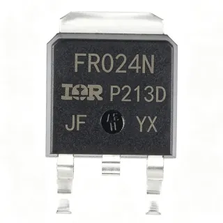
IRLR3636TRLPBF - 60V 99A N-Ch IR MOSFET, DPAK | Infineon
MPN: IRLR3636TRLPBF ✓ Active| Qty | Unit Price | Extended |
|---|---|---|
| 1 | $1.83 | $1.83 |
| 10 | $1.65 | $16.50 |
| 100 | $1.32 | $132.00 |
| 500 | $1.08 | $540.00 |
| 1,000 | $0.89 | $890.00 |
| 3,000 | $0.74 | $2,220.00 |
IRLR3636TRLPBF Overview
A power MOSFET is a voltage-controlled semiconductor switch that uses an insulated gate to modulate current flow between drain and source terminals. The IRLR3636TRLPBF belongs to the N-channel enhancement-mode MOSFET family, where applying a positive gate-source voltage creates an inversion layer that conducts current. As part of the broader MOSFET → power transistor → discrete semiconductor → semiconductor taxonomy, it sits in the voltage-regulator/synchronous-rectification segment of power electronics where low RDS(on) and fast switching directly impact efficiency.
Key features of the IRLR3636TRLPBF include 6.8 mΩ maximum RDS(on), 99 A peak ID, logic-level gate threshold (VGS(th) around 1.0-2.5 V), avalanche-rated body diode, and 33 nC total gate charge. The low on-resistance minimises conduction losses, while the small QG reduces switching losses at high frequencies, collectively improving system efficiency in SMPS and motor-drive applications.
The device uses Infineon's advanced IR process technology, combining a trench MOSFET architecture with a ruggedised die layout. This produces a low figure-of-merit (FOM = RDS(on) × QG) and robust avalanche capability. The DPAK package provides a low thermal resistance path via its exposed drain tab, which doubles as the mounting surface for heat-sinking to the PCB copper pour.
Typical applications include DC motor drives, high-efficiency synchronous rectification in switch-mode power supplies (SMPS), uninterruptible power supplies (UPS), and high-speed power switching in hard-switched topologies. The logic-level gate makes it directly compatible with 5 V microcontroller outputs without a dedicated gate driver in lower-power circuits.
When designing with this MOSFET, ensure that the gate drive voltage stays within the absolute-maximum VGS rating of ±20 V (or ±16 V per some datasheet sources). PCB layout should minimise the source-inductance loop; place the gate driver physically close to the gate pin and use a Kelvin-source connection where possible.
This page synthesises distributor pricing, drop-in alternatives, and practical design notes that go beyond the manufacturer datasheet alone, giving engineers a single reference for selecting and qualifying this part.
Drop-in alternatives for IRLR3636TRLPBF — same package, pin-to-pin compatible. Different-package parts requiring PCB rework are excluded.
Variants in this series
Same-series models that are drop-in compatible with IRLR3636TRLPBF (same form factor and footprint) — differing in Technology, Package, FET Type, Operating Temperature Range, Total Gate Charge (Qg).
Quick Comparison Tool — Select alternative parts for side-by-side comparison:
IRLR3636PBF
✅ Drop-In📋 Reference alternative (not in catalog)
IRLR3636TRPBF
✅ Drop-In✓ In Stock
$2.38 / Unit
View Datasheet →AUIRLR3636
✅ Drop-In📋 Reference alternative (not in catalog)
IRLR3410TRPBF
✅ Drop-In✓ In Stock
$0.81 / Unit
View Datasheet →IRLR3114ZTRPBF
✅ Drop-In✓ In Stock
$0.46 / Unit
View Datasheet →IRLR2905TRPBF
✅ Drop-In✓ In Stock
$0.61 / Unit
View Datasheet →IRLR3636TRLPBF Maximum Ratings & Electrical Characteristics
| FET Type | N-Channel MOSFET |
| Technology | IR HEXFET® (IR MOSFET™) |
| Drain-to-Source Voltage (VDS) | 60 V |
| Continuous Drain Current (ID, TC=25°C) | 50 A |
| RDS(on) Max @ VGS=10V | 6.8 mΩ |
| Gate-to-Source Voltage (VGS) Max | ±20 V |
| Gate Threshold Voltage (VGS(th)) | 1.0 V to 2.5 V (logic-level) |
| Total Gate Charge (QG) | 33 nC |
| Power Dissipation (PD, TC=25°C) | 143 W |
| Operating Temperature Range | -55 °C to +175 °C (TJ) |
| Package | TO-252AA (DPAK) |
| Mounting Type | Surface Mount |
| Lead-Free / RoHS | Yes (PBF suffix) |
| Avalanche Rated | Yes (per Infineon datasheet family) |
IRLR3636TRLPBF Pin Configuration
| Pin 1 | Gate — Gate drive input (logic-level, VGS(th) 1.0-2.5 V) |
| Pin 2 | Drain (Tab) — Drain output, internally connected to the mounting tab; tab is the primary thermal dissipation path |
| Pin 3 | Source — Source return, connect to system ground (or low-side shunt) |
Safe Operating Area (DC, TC=25°C)
Typical Applications
IRLR3636TRLPBF is suitable for 6 applications: DC Motor Drive (H-Bridge / Half-Bridge), Synchronous Rectification in SMPS, Uninterruptible Power Supply (UPS) Battery Switch, High-Side/Low-Side Power Switching in E-Bike / E-Scooter, Solar Charge Controller / Battery Management, Industrial Solenoid / Relay Driver.
DC Motor Drive (H-Bridge / Half-Bridge)
The IRLR3636TRLPBF is well-suited to 12-48 V brushed DC motor drive half-bridges and H-bridges. Its 60 V VDS rating provides adequate headroom for inductive flyback transients in 24 V and 36 V battery-powered systems, while the 6.8 mΩ RDS(on) at logic-level VGS minimises conduction loss during PWM operation at high duty cycle. The DPAK package's exposed drain tab ties directly to a copper pour, enabling continuous currents above 30 A without forced-air cooling. Designers should add a snubber or TVS clamp across the drain-source to absorb avalanche energy during motor commutation.
Recommended
Synchronous Rectification in SMPS
As a synchronous rectifier on the secondary side of an isolated SMPS, the IRLR3636TRLPBF's low RDS(on) of 6.8 mΩ and 33 nC total gate charge deliver a figure-of-merit that approaches efficiency limits for 12 V output rails. Replacing Schottky diodes in 5 V to 12 V buck-derived converters reduces forward-conduction loss from ~0.5 V to a few mV at full load. The logic-level gate allows direct drive from a sync-rectifier controller IC such as the NCP4306. Engineers should observe the body-diode reverse-recovery characteristic when used in hard-switched topologies above 100 kHz.
Recommended
Uninterruptible Power Supply (UPS) Battery Switch
In line-interactive and online UPS designs, the IRLR3636TRLPBF serves as the low-side disconnect switch between the battery bank and the DC bus, or as part of a bidirectional buck-boost converter for battery charging/discharging. Its 50 A continuous drain rating handles typical 1-2 kVA UPS battery currents with margin, and the 60 V VDS covers 48 V battery stacks including transient surges. The DPAK package enables compact PCB layouts in 1U rack-mounted UPS form factors. A pre-charge resistor plus NTC thermistor is recommended to limit inrush current at hot-plug events.
Recommended
High-Side/Low-Side Power Switching in E-Bike / E-Scooter
The IRLR3636TRLPBF functions as the low-side PWM switch or synchronous FET in 24-36 V e-bike controller boards. Its logic-level gate drive allows direct connection to a 3.3 V or 5 V MCU PWM output through a small gate resistor, eliminating a discrete gate driver in cost-sensitive designs. The 6.8 mΩ RDS(on) keeps conduction loss manageable for motor currents up to 25 A continuous, while the rugged DPAK package withstands the vibration and thermal cycling typical of personal-electric-vehicle duty profiles.
Recommended
Solar Charge Controller / Battery Management
In MPPT or PWM solar charge controllers for off-grid photovoltaic systems, the IRLR3636TRLPBF operates as the main switching element in the buck converter between the PV panel (open-circuit up to ~45 V in 24 V systems) and the battery bus. Its 60 V VDS handles 24 V panel Voc with margin, while the low RDS(on) reduces thermal stress during continuous 30-40 A charge currents. The part's avalanche rating also tolerates the inductive ringing from long PV-cable inductance during MPPT step changes.
Recommended
Industrial Solenoid / Relay Driver
The IRLR3636TRLPBF is a robust low-side driver for 24 V industrial solenoid valves, pneumatic actuators, and relay coils. Each FET can switch several amps of inductive load current with logic-level control from a PLC output or industrial microcontroller. The 60 V VDS comfortably clamps the inductive kickback when combined with a flyback diode or TVS clamp, and the DPAK package dissipates the average coil current without a heatsink in many cases. For multi-channel solenoid banks, paralleling multiple IRLR3636TRLPBF devices shares current and reduces per-channel RDS(on).
Recommended
Recommended Products Summary
Engineering reference data for IRLR3636TRLPBF — comparison, design guidance, and compliance information.
Selection Guide
Comparison with Alternatives
| Parameter | This Product | IRLR3636PBF | AUIRLR3636 | IRLR3410TRPBF | IRLR3114ZTRPBF |
|---|---|---|---|---|---|
| Brand | Infineon Technologies | Infineon Technologies | Infineon Technologies | Infineon Technologies | Infineon Technologies |
| Package | TO-252AA (DPAK) | TO-252AA (DPAK) - same | TO-252AA (DPAK) - same | TO-252AA (DPAK) - same | TO-252AA (DPAK) - same |
| Drain-Source Voltage (VDS) | 60 V | 60 V | 60 V | 100 V | 40 V |
| Continuous Drain Current (ID, TC=25°C) | 50 A | 50 A | 50 A | 30 A | 40 A |
| RDS(on) Max @ VGS=10V | 6.8 mΩ | 6.8 mΩ | 6.8 mΩ | 28 mΩ | 3.2 mΩ |
| Gate Threshold (VGS(th)) | 1.0 V to 2.5 V (logic-level) | 1.0 V to 2.5 V | 1.0 V to 2.5 V | 1.0 V to 2.5 V | 1.0 V to 2.5 V |
| Total Gate Charge (QG) | 33 nC | 33 nC | 33 nC | 48 nC | 24 nC |
| Power Dissipation (PD) | 143 W | 143 W | 143 W | 120 W | 130 W |
| Automotive Grade | No (industrial) | No | Yes (AEC-Q101) | No | No |
Key Differentiators
- Lower RDS(on) than higher-voltage family parts (vs IRLR3410TRPBF)
- Logic-level gate drive compatible with 5V MCU (vs IRLR3114ZTRPBF)
- Automotive-qualified option available on same die (vs AUIRLR3636)
Design Notes
Estimated: At continuous drain current of 30 A with RDS(on) = 6.8 mΩ, conduction loss is approximately P = I² × RDS(on) = 30² × 0.0068 ≈ 6.1 W. The TO-252 DPAK package has theta_JA ≈ 50 °C/W on a 1 oz single-sided 1 sq-inch copper pad, giving a junction temperature rise of ~305 °C - clearly above the 175 °C limit. For 30 A continuous operation, the design must use a minimum 4 sq-inch copper pour on both sides of the PCB, or attach an external heatsink. Derate to ~15-20 A continuous without a heatsink on a typical 2-layer FR4 board.
The DPAK drain tab doubles as the thermal pad and must be soldered to a substantial copper pour for heat dissipation. Recommended land pattern per IPC-7351: drain pad 6.5 mm × 5.5 mm minimum, gate and source pads 1.5 mm × 1.0 mm with 0.5 mm pitch. Use thermal vias (0.3 mm diameter, 1 mm pitch) under the drain pad to inner copper planes. Gate-drive traces should be kept short (<10 mm) to minimise gate-loop inductance and prevent ringing during fast switching edges.
Three common pitfalls with this part: (1) Do not exceed VGS absolute maximum of ±20 V; use a gate-source Zener clamp (e.g. 15 V) when driving from a 12 V or higher rail. (2) The body diode reverse-recovery (Qrr) is significant in hard-switched topologies above 100 kHz - consider Infineon StrongIRFET or OptiMOS alternatives for >200 kHz designs. (3) In parallel operation, source-inductance mismatch causes uneven current sharing; use a Kelvin-source connection with individual gate resistors per FET rather than a shared gate resistor.
In buck-converter or half-bridge layouts, minimise the high-side/low-side drain-source switching loop by placing the input decoupling capacitor directly between the high-side drain and low-side source. Keep the gate-drive loop area below 5 mm² to limit parasitic inductance below 5 nH. Use a ground plane on the bottom layer stitched with vias around the switching node to contain EMI. The source pin (pin 3) should connect to the system ground plane at a single point near the gate-driver return to avoid high-current return paths coupling into the gate drive signal.
Compliance Information
PBF suffix confirms Pb-free and RoHS compliance per Infineon datasheet. Not AEC-Q100 qualified (use AUIRLR3636 for automotive). REACH compliance declared by Infineon. Halogen-free status not explicitly confirmed in verified data.